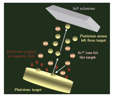
Semiconductor Type Dependent Comparison of Electrical Characteristics of Pt/InP Structures Fabricated by Magnetron Sputtering Technique in the Range of 20–400 K
Corresponding Author: H. Korkut
Nano-Micro Letters,
Vol. 5 No. 1 (2013), Article Number: 34-39
Abstract
The paper describes how electrical properties of Pt/InP Schottky diode were affected by semiconductor type. We fabricated Pt/p-InP and Pt/n-InP Schottky diodes and measured electrical characteristics from 20 K to 400 K. Thicknesses of less than 30 nm of platinum were deposited on the two types of indium phosphide substrates using magnetron sputtering technique after the creation of Zn-Au ohmic back contact. We discussed basic diode parameters of idealiy factors, barrier heights and serries resistances of the two type of contacts. Additionly, unusual temperature characteristics of the the diodes were highlighted. These results were evaluated in terms of semiconductor type comparision of Pt/InP Schottky structures.
Keywords
Download Citation
Endnote/Zotero/Mendeley (RIS)BibTeX
- A. Akbay, H. Korkut, K. Ejderha, T. Korkut and A. Türüt, “Responses of Pt/n-InP Schottky diode to electron irradiation in different temperature conditions”, J. Radioanal. Nucl. Chem. 289(1), 145–148 (2011). http://dx.doi.org/10.1007/s10967-011-1041-y
- P. Veeramani, M. Haris and S. M. Babu, “Investigation of CdTex and Cd1-xZnxTe Schottky barrier diode structure based γ-ray detectors”, Mater. Manufact. Proc, 22(3), 375–378 (2007). http://dx.doi.org/10.1080/10426910701190873
- D. E. Yildiz, Ş. Altindal, Z. Tekeli and M. Özer, “The effects of surface states and series resistance on the performance of Au/SnO2/n-Si and Al/SnO2/p-Si (MIS) Schottky barrier diodes”, Mat. Sci. Semicon. Proc. 13(1), 34–40 (2010). http://dx.doi.org/10.1016/j.mssp.2010.02.004
- M. Siad, A. Keffous, S. Mamma, Y. Belkacem and H. Menari, “Correlation between series resistance and parameters of Al/n-Si and Al/p-Si Schottky barrier diodes”, Appl. Surf. Sci. 236(1–4), 366–376 (2004). http://dx.doi.org/10.1016/j.apsusc.2004.05.009
- K. Akkiliç, A. Türüt, G. Çankaya and T. Kiliçoğlu, “Correlation between barrier heights and ideality factors of Cd/n-Si and Cd/p-Si Schottky barrier diodes” Solid State Commun. 125(10), 551–556 (2003). http://dx.doi.org/10.1016/S0038-1098(02)00829-3
- E. Arslan, H. Çakmak and E. Özbay, “Forward tunneling current in Pt/p-InGaN and Pt/n-InGaN Schottky barriers in a wide temperature range” Microelectron. Eng. 100, 51–56 (2012). http://dx.doi.org/10.1016/j.mee.2012.07.103
- K. Kaneto and W. Takashima, “Fabrication and characteristics of Schottky diodes based on regioregular poly (3-hexylthiophene)/Al junction”, Curr. Appl. Phys. 1(4-5), 355–361 (2001). http://dx.doi.org/10.1016/S1567-1739(01)00035-9
- S. Chand and S. Bala, “Analysis of current-voltage characteristics of inhomogeneous Schottky diodes at low temperatures”, Appl. Surf. Sci. 252(2), 358–363 (2005). http://dx.doi.org/10.1016/j.apsusc.2005.01.009
- J. Osvald and Zs. Horvath, “Theoretical study of the temperature dependence of electrical characteristics of Schottky diodes with an inverse near-surface layer”, J. Appl. Surf. Sci. 234(1–4), 349–354 (2004). http://dx.doi.org/10.1016/j.apsusc.2004.05.046
- H. Norde, “A modified forward I-V plot for Schottky diodes with high series resistance”, J. Appl. Phys. 50, 5052–5053 (1979). http://dx.doi.org/10.1063/1.325607
- A. B. Mcleon, “Limitations to the Norde I-V plot”, Semicond. Sci. Technol. 1, 177–179 (1986). http://dx.doi.org/10.1088/0268-1242/1/3/003
References
A. Akbay, H. Korkut, K. Ejderha, T. Korkut and A. Türüt, “Responses of Pt/n-InP Schottky diode to electron irradiation in different temperature conditions”, J. Radioanal. Nucl. Chem. 289(1), 145–148 (2011). http://dx.doi.org/10.1007/s10967-011-1041-y
P. Veeramani, M. Haris and S. M. Babu, “Investigation of CdTex and Cd1-xZnxTe Schottky barrier diode structure based γ-ray detectors”, Mater. Manufact. Proc, 22(3), 375–378 (2007). http://dx.doi.org/10.1080/10426910701190873
D. E. Yildiz, Ş. Altindal, Z. Tekeli and M. Özer, “The effects of surface states and series resistance on the performance of Au/SnO2/n-Si and Al/SnO2/p-Si (MIS) Schottky barrier diodes”, Mat. Sci. Semicon. Proc. 13(1), 34–40 (2010). http://dx.doi.org/10.1016/j.mssp.2010.02.004
M. Siad, A. Keffous, S. Mamma, Y. Belkacem and H. Menari, “Correlation between series resistance and parameters of Al/n-Si and Al/p-Si Schottky barrier diodes”, Appl. Surf. Sci. 236(1–4), 366–376 (2004). http://dx.doi.org/10.1016/j.apsusc.2004.05.009
K. Akkiliç, A. Türüt, G. Çankaya and T. Kiliçoğlu, “Correlation between barrier heights and ideality factors of Cd/n-Si and Cd/p-Si Schottky barrier diodes” Solid State Commun. 125(10), 551–556 (2003). http://dx.doi.org/10.1016/S0038-1098(02)00829-3
E. Arslan, H. Çakmak and E. Özbay, “Forward tunneling current in Pt/p-InGaN and Pt/n-InGaN Schottky barriers in a wide temperature range” Microelectron. Eng. 100, 51–56 (2012). http://dx.doi.org/10.1016/j.mee.2012.07.103
K. Kaneto and W. Takashima, “Fabrication and characteristics of Schottky diodes based on regioregular poly (3-hexylthiophene)/Al junction”, Curr. Appl. Phys. 1(4-5), 355–361 (2001). http://dx.doi.org/10.1016/S1567-1739(01)00035-9
S. Chand and S. Bala, “Analysis of current-voltage characteristics of inhomogeneous Schottky diodes at low temperatures”, Appl. Surf. Sci. 252(2), 358–363 (2005). http://dx.doi.org/10.1016/j.apsusc.2005.01.009
J. Osvald and Zs. Horvath, “Theoretical study of the temperature dependence of electrical characteristics of Schottky diodes with an inverse near-surface layer”, J. Appl. Surf. Sci. 234(1–4), 349–354 (2004). http://dx.doi.org/10.1016/j.apsusc.2004.05.046
H. Norde, “A modified forward I-V plot for Schottky diodes with high series resistance”, J. Appl. Phys. 50, 5052–5053 (1979). http://dx.doi.org/10.1063/1.325607
A. B. Mcleon, “Limitations to the Norde I-V plot”, Semicond. Sci. Technol. 1, 177–179 (1986). http://dx.doi.org/10.1088/0268-1242/1/3/003

