Nanoimprint Lithography Enabling High-Performance Organic Optoelectronics: Advances and Perspectives

Corresponding Author: Tianrui Zhai
Nano-Micro Letters,
Vol. 18 (2026), Article Number: 236
Abstract
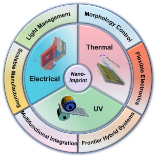
Organic optoelectronic devices demonstrate immense potential in flexible displays, wearable electronics, and artificial skin, needing precise light-field and morphology management strategies to further improve their opto-electric performance. Nanoimprint lithography (NIL) has emerged as a high-resolution, high-efficiency, and low-cost patterning technique that mechanically transferring micro/nanoscale patterns from a template to a substrate to significantly enhance the optoelectronic performance through the precise creation of advanced light-management structures, combined with additional solid-state stacking morphology. This review systematically summarizes recent advances in NIL technology for organic optoelectronics. It begins with an introduction to the fundamental principles, main process variants (thermal, ultraviolet, and electrochemical NIL), as well as key technical issues. Subsequently, through specific applications in organic light-emitting diodes, organic solar cells, and organic field-effect transistors, it highlights the exceptional capabilities of NIL to enhance device performance by controlling crystallization and creating functional micro/nanostructuring. Specific advantages include enabling high-efficiency light management to overcome efficiency bottlenecks, facilitating low-cost, high-throughput manufacturing for industrialization, full compatibility with flexible substrates for emerging applications, enabling multifunctional integration and novel device architectures, and tailoring material microstructures and properties advance fundamental research. Finally, we discuss the remaining challenges and future prospects of NIL in integrated organic optoelectronic systems.
Highlights:
1 Nanoimprint lithography (NIL) enables high-performance light management in organic light-emitting diodes and organic solar cells, and enhances charge transport in organic field-effect transistors via controlled molecular ordering, pushing organic optoelectronics beyond conventional efficiency limits.
2 The technology provides a scalable, low-cost platform for large-area fabrication on flexible substrates, effectively bridging the gap between laboratory innovation and industrial mass production.
3 NIL uniquely empowers the creation of multifunctional integrated devices and novel architectures, opening pathways for next-generation wearable electronics and bio-integrated systems.
Keywords
Download Citation
Endnote/Zotero/Mendeley (RIS)BibTeX
- S. Chang, J.H. Koo, J. Yoo, M.S. Kim, M.K. Choi et al., Flexible and stretchable light-emitting diodes and photodetectors for human-centric optoelectronics. Chem. Rev. 124(3), 768–859 (2024). https://doi.org/10.1021/acs.chemrev.3c00548
- X. Wu, S. Ni, C.-H. Wang, W. Zhu, P.-T. Chou, Comprehensive review on the structural diversity and versatility of multi-resonance fluorescence emitters: advance, challenges, and prospects toward OLEDs. Chem. Rev. 125(14), 6685–6752 (2025). https://doi.org/10.1021/acs.chemrev.3c00847
- Y. Huang, E.-L. Hsiang, M.-Y. Deng, S.-T. Wu, Mini-LED, Micro-LED and OLED displays: present status and future perspectives. Light Sci. Appl. 9, 105 (2020). https://doi.org/10.1038/s41377-020-0341-9
- Y. Shi, M. Sun, H. Shi, Z. Liang, B. Qiao et al., Integrating AI into OLED material design: a comprehensive review of computational frameworks, challenges, and opportunities. Sci. Bull. 70(18), 3058–3089 (2025). https://doi.org/10.1016/j.scib.2025.07.007
- S. Liu, C. Zang, J. Zhang, S. Tian, Y. Wu et al., Air-stable ultrabright inverted organic light-emitting devices with metal ion-chelated polymer injection layer. Nano-Micro Lett. 14(1), 14 (2021). https://doi.org/10.1007/s40820-021-00745-w
- H.-W. Chen, J.-H. Lee, B.-Y. Lin, S. Chen, S.-T. Wu, Liquid crystal display and organic light-emitting diode display: present status and future perspectives. Light Sci. Appl. 7, 17168 (2018). https://doi.org/10.1038/lsa.2017.168
- N. Song, J. Xue, Y. Chen, X. Xin, J. Wu et al., Meniscus-guided molecular alignment for high-efficiency solution-processed DR/NIR-OLEDs. Adv. Opt. Mater. 13(25), e01346 (2025). https://doi.org/10.1002/adom.202501346
- Y. Zhang, H. Xia, J. Yu, Y. Yang, G. Li, Materials and device engineering perspective: recent advances in organic photovoltaics. Adv. Mater. 37(48), 2504063 (2025). https://doi.org/10.1002/adma.202504063
- S. Park, S.W. Heo, W. Lee, D. Inoue, Z. Jiang et al., Self-powered ultra-flexible electronics via nano-grating-patterned organic photovoltaics. Nature 561(7724), 516–521 (2018). https://doi.org/10.1038/s41586-018-0536-x
- S. Zhang, L. Ye, H. Zhang, J. Hou, Green-solvent-processable organic solar cells. Mater. Today 19(9), 533–543 (2016). https://doi.org/10.1016/j.mattod.2016.02.019
- L. Wei, Y. Yang, L. Zhan, S. Yin, H. Chen, Optimizing exciton and charge-carrier behavior in thick-film organic photovoltaics: a comprehensive review. Nano-Micro Lett. 18(1), 10 (2025). https://doi.org/10.1007/s40820-025-01852-8
- N. Liang, R. Tian, Y. Xu, H. Yao, H. Yang et al., Trans-reflective structural color filters assisting multifunctional-integrated semitransparent photovoltaic window. Adv. Mater. 35(22), e2300360 (2023). https://doi.org/10.1002/adma.202300360
- Y.-B. Cheng, A. Pascoe, F. Huang, Y. Peng, Print flexible solar cells. Nature 539(7630), 488–489 (2016). https://doi.org/10.1038/539488a
- T. Liu, M.M.S. Almutairi, J. Ma, A. Stewart, Z. Xing et al., Solution-processed thin film transparent photovoltaics: present challenges and future development. Nano-Micro Lett. 17(1), 49 (2024). https://doi.org/10.1007/s40820-024-01547-6
- G. Dastgeer, M.W. Zulfiqar, S. Nisar, R. Zulfiqar, M. Imran et al., Emerging role of 2D materials in photovoltaics: efficiency enhancement and future perspectives. Nano-Micro Lett. 18(1), 32 (2025). https://doi.org/10.1007/s40820-025-01869-z
- M. Li, M. Rogatch, H. Chen, X. Guo, J. Tang, Supramolecular design and assembly engineering toward high-performance organic field-effect transistors. Acc. Mater. Res. 5(4), 505–517 (2024). https://doi.org/10.1021/accountsmr.4c00009
- W. Wang, L. Wang, G. Dai, W. Deng, X. Zhang et al., Controlled growth of large-area aligned single-crystalline organic nanoribbon arrays for transistors and light-emitting diodes driving. Nano-Micro Lett. 9(4), 52 (2017). https://doi.org/10.1007/s40820-017-0153-5
- T. Yang, Q. Wu, F. Dai, K. Huang, H. Xu et al., Understanding, optimizing, and utilizing nonideal transistors based on organic or organic hybrid semiconductors. Adv. Funct. Mater. 30(20), 1903889 (2020). https://doi.org/10.1002/adfm.201903889
- Y. Wang, S. Sun, Y. Huang, Y. Fu, J. Qi et al., Grain boundary engineering of organic semiconductor films in organic transistors. Aggregate 4(6), e379 (2023). https://doi.org/10.1002/agt2.379
- S. Cui, K. Sun, Z. Liao, Q. Zhou, L. Jin et al., Flexible nanoimprint lithography enables high-throughput manufacturing of bioinspired microstructures on warped substrates for efficient III-nitride optoelectronic devices. Sci. Bull. 69(13), 2080–2088 (2024). https://doi.org/10.1016/j.scib.2024.04.030
- Z. Shen, W. Huang, L. Li, H. Li, J. Huang et al., Research progress of organic field-effect transistor based chemical sensors. Small 19(41), 2302406 (2023). https://doi.org/10.1002/smll.202302406
- H. Dong, X. Fu, J. Liu, Z. Wang, W. Hu, 25th anniversary : key points for high-mobility organic field-effect transistors. Adv. Mater. 25(43), 6158–6183 (2013). https://doi.org/10.1002/adma.201302514
- M. Li, J. Zheng, X. Wang, R. Yu, Y. Wang et al., Light-responsive self-strained organic semiconductor for large flexible OFET sensing array. Nat. Commun. 13(1), 4912 (2022). https://doi.org/10.1038/s41467-022-32647-9
- C. Grivas, M. Pollnau, Organic solid-state integrated amplifiers and lasers. Laser Photonics Rev. 6(4), 419–462 (2012). https://doi.org/10.1002/lpor.201100034
- G. Xie, L. Ding, Triplet manipulation for strong luminescence. Sci. Bull. 65(21), 1780–1782 (2020). https://doi.org/10.1016/j.scib.2020.07.004
- Y. Jiang, Y.-Y. Liu, X. Liu, H. Lin, K. Gao et al., Organic solid-state lasers: a materials view and future development. Chem. Soc. Rev. 49, 5885–5944 (2020). https://doi.org/10.1039/d0cs00037j
- L. Wang, Z. Zhao, G. Zhan, H. Fang, H. Yang et al., Deep-blue organic light-emitting diodes based on a doublet d-f transition cerium(III) complex with 100% exciton utilization efficiency. Light Sci. Appl. 9, 157 (2020). https://doi.org/10.1038/s41377-020-00395-4
- M.A. Fusella, R. Saramak, R. Bushati, V.M. Menon, M.S. Weaver et al., Plasmonic enhancement of stability and brightness in organic light-emitting devices. Nature 585(7825), 379–382 (2020). https://doi.org/10.1038/s41586-020-2684-z
- S. Kim, J. Seo, J. Choi, H. Yoo, Vertically integrated electronics: new opportunities from emerging materials and devices. Nano-Micro Lett. 14(1), 201 (2022). https://doi.org/10.1007/s40820-022-00942-1
- W. Shi, Y. Guo, Y. Liu, When flexible organic field-effect transistors meet biomimetics: a prospective view of the internet of things. Adv. Mater. 32(15), e1901493 (2020). https://doi.org/10.1002/adma.201901493
- J. Yu, J. Pu, D. Xie, Z. Ai, Y. Lang et al., Semitransparent organic photovoltaics with wide geographical adaptability as sustainable smart windows. Nat. Commun. 16(1), 7421 (2025). https://doi.org/10.1038/s41467-025-62546-8
- Y. Chen, X. Wu, Y. Chu, J. Zhou, B. Zhou et al., Hybrid field-effect transistors and photodetectors based on organic semiconductor and CsPbI3 perovskite nanorods bilayer structure. Nano-Micro Lett. 10(4), 57 (2018). https://doi.org/10.1007/s40820-018-0210-8
- A. Moreno, D. Chemisana, E.F. Fernández, Energy performance and crop yield production of a semitransparent photovoltaic greenhouse. Appl. Energy 382, 125285 (2025). https://doi.org/10.1016/j.apenergy.2025.125285
- H. Huang, Y. Wu, Y. Ma, P. Xue, Y. Cao et al., Synergistic approach of energy generation and conservation in buildings exploiting semitransparent organic photovoltaic windows globally. Nano Energy 142, 111181 (2025). https://doi.org/10.1016/j.nanoen.2025.111181
- K. Yoshida, C. Chen, H. Haas, G.A. Turnbull, I.D.W. Samuel, RGB-single-chip OLEDs for high-speed visible-light communication by wavelength-division multiplexing. Adv. Sci. 11(47), 2404576 (2024). https://doi.org/10.1002/advs.202404576
- D. Kim, H.-J. Park, S.-H. Jung, W.J. Pyo, S.Z. Hassan et al., Visible-light communication with lighting: RGB wavelength division multiplexing OLEDs/OPDs platform. Adv. Mater. 36(4), e2309416 (2024). https://doi.org/10.1002/adma.202309416
- M. Riahi, K. Yoshida, I.D.W. Samuel, Improving the air stability of flexible top-emitting organic light-emitting diodes. NPJ Flex. Electron. 8, 51 (2024). https://doi.org/10.1038/s41528-024-00338-8
- K.-W. Lee, Y. Wan, Z. Huang, Q. Zhao, S. Li et al., Organic optoelectronic materials: a rising star of bioimaging and phototherapy. Adv. Mater. 36(17), 2306492 (2024). https://doi.org/10.1002/adma.202306492
- X. Rodríguez-Martínez, S. Riera-Galindo, L.E. Aguirre, M. Campoy-Quiles, H. Arwin et al., Laminated organic photovoltaic modules for agrivoltaics and beyond: an outdoor stability study of all-polymer and polymer: small molecule blends. Adv. Funct. Mater. 33(10), 2213220 (2023). https://doi.org/10.1002/adfm.202213220
- A. Yin, J. Wang, S. Hu, M. Sun, B. Sun et al., High performance waterproof-breathable fully flexible tactile sensor based on piezotronics coupled OFET. Nano Energy 106, 108034 (2023). https://doi.org/10.1016/j.nanoen.2022.108034
- X. Wu, S. Mao, J. Chen, J. Huang, Strategies for improving the performance of sensors based on organic field-effect transistors. Adv. Mater. 30(17), e1705642 (2018). https://doi.org/10.1002/adma.201705642
- J. Ge, B. Ding, S. Hou, M. Luo, D. Nam et al., Rapid fabrication of complex nanostructures using room-temperature ultrasonic nanoimprinting. Nat. Commun. 12(1), 3146 (2021). https://doi.org/10.1038/s41467-021-23427-y
- S. He, Y. Tian, H. Zhou, M. Zhu, C. Li et al., Review for micro-nano processing technology of microstructures and metadevices. Adv. Funct. Mater. 35(24), 2420369 (2025). https://doi.org/10.1002/adfm.202420369
- Z. Liu, N. Liu, J. Schroers, Nanofabrication through molding. Prog. Mater. Sci. 125, 100891 (2022). https://doi.org/10.1016/j.pmatsci.2021.100891
- S.Y. Chou, P.R. Krauss, P.J. Renstrom, Imprint of sub-25 nm vias and trenches in polymers. Appl. Phys. Lett. 67(21), 3114–3116 (1995). https://doi.org/10.1063/1.114851
- X. Lu, X. Wang, S. Wang, T. Ding, Polarization-directed growth of spiral nanostructures by laser direct writing with vector beams. Nat. Commun. 14, 1422 (2023). https://doi.org/10.1038/s41467-023-37048-0
- S.T. Zimmermann, D.W.R. Balkenende, A. Lavrenova, C. Weder, J. Brugger, Nanopatterning of a stimuli-responsive fluorescent supramolecular polymer by thermal scanning probe lithography. ACS Appl. Mater. Interfaces 9(47), 41454–41461 (2017). https://doi.org/10.1021/acsami.7b13672
- Z. Gan, H. Feng, L. Chen, S. Min, C. Liang et al., Spatial modulation of nanopattern dimensions by combining interference lithography and grayscale-patterned secondary exposure. Light Sci. Appl. 11, 89 (2022). https://doi.org/10.1038/s41377-022-00774-z
- M. Grzelczak, J. Vermant, E.M. Furst, L.M. Liz-Marzán, Directed self-assembly of nanops. ACS Nano 10(7), 3591–3605 (2010). https://doi.org/10.1021/nn100869j
- W. Qiao, W. Huang, Y. Liu, X. Li, L.-S. Chen et al., Toward scalable flexible nanomanufacturing for photonic structures and devices. Adv. Mater. 28(47), 10353–10380 (2016). https://doi.org/10.1002/adma.201601801
- C. Wang, J. Shao, H. Tian, X. Li, Y. Ding et al., Step-controllable electric-field-assisted nanoimprint lithography for uneven large-area substrates. ACS Nano 10(4), 4354–4363 (2016). https://doi.org/10.1021/acsnano.5b08032
- Y. Yang, Y. Jeon, Z. Dong, J.K.W. Yang, M. Haddadi Moghaddam et al., Nanofabrication for nanophotonics. ACS Nano 19(13), 12491–12605 (2025). https://doi.org/10.1021/acsnano.4c10964
- J. Shao, X. Chen, X. Li, H. Tian, C. Wang et al., Nanoimprint lithography for the manufacturing of flexible electronics. Sci. China Technol. Sci. 62(2), 175–198 (2019). https://doi.org/10.1007/s11431-018-9386-9
- J. Zhang, S. Jirigalantu, Y. Yu, HYu. Wang et al., Research on manufacturing technology of nanoimprinted grating. J. Manuf. Process. 131, 891–909 (2024). https://doi.org/10.1016/j.jmapro.2024.09.033
- Z. Wang, S. Guo, H. Li, B. Wang, Y. Sun et al., The semiconductor/conductor interface piezoresistive effect in an organic transistor for highly sensitive pressure sensors. Adv. Mater. 31(6), 1805630 (2019). https://doi.org/10.1002/adma.201805630
- S.-X. Li, G.-Y. Huang, H. Xia, T. Fu, X.-J. Wang et al., Nanoimprint crystalithography for organic semiconductors. Nat. Commun. 16, 3636 (2025). https://doi.org/10.1038/s41467-025-58934-9
- Y. Zhang, C.-T. Lin, S. Yang, Fabrication of hierarchical pillar arrays from thermoplastic and photosensitive SU-8. Small 6(6), 768–775 (2010). https://doi.org/10.1002/smll.200901843
- M.-G. Kang, M.-S. Kim, J. Kim, L.J. Guo, Organic solar cells using nanoimprinted transparent metal electrodes. Adv. Mater. 20(23), 4408–4413 (2008). https://doi.org/10.1002/adma.200800750
- W. Zhou, G. Min, J. Zhang, Y. Liu, J. Wang et al., Nanoimprint lithography: a processing technique for nanofabrication advancement. Nano-Micro Lett. 3(2), 135–140 (2011). https://doi.org/10.1007/BF03353663
- S.Y. Chou, P.R. Krauss, P.J. Renstrom, Imprint lithography with 25-nanometer resolution. Science 272(5258), 85–87 (1996). https://doi.org/10.1126/science.272.5258.85
- M. Colburn, S.C. Johnson, M.D. Stewart, S. Damle, T.C. Bailey et al., Step and flash imprint lithography: a new approach to high-resolution patterning. Emerging Lithographic Technologies III. Santa Clara, CA. SPIE, (1999). pp. 379. https://doi.org/10.1117/12.351155
- M. Aryal, K. Trivedi, W. Hu, Nano-confinement induced chain alignment in ordered P3HT nanostructures defined by nanoimprint lithography. ACS Nano 3(10), 3085–3090 (2009). https://doi.org/10.1021/nn900831m
- S.H. Ahn, L.J. Guo, Large-area roll-to-roll and roll-to-plate nanoimprint lithography: a step toward high-throughput application of continuous nanoimprinting. ACS Nano 3(8), 2304–2310 (2009). https://doi.org/10.1021/nn9003633
- W.-J. Joo, J. Kyoung, M. Esfandyarpour, S.-H. Lee, H. Koo et al., Metasurface-driven OLED displays beyond 10,000 pixels per inch. Science 370(6515), 459–463 (2020). https://doi.org/10.1126/science.abc8530
- K. Yoshida, J. Gong, A.L. Kanibolotsky, P.J. Skabara, G.A. Turnbull et al., Electrically driven organic laser using integrated OLED pumping. Nature 621(7980), 746–752 (2023). https://doi.org/10.1038/s41586-023-06488-5
- M. Modaresialam, Z. Chehadi, T. Bottein, M. Abbarchi, D. Grosso, Nanoimprint lithography processing of inorganic-based materials. Chem. Mater. 33(14), 5464–5482 (2021). https://doi.org/10.1021/acs.chemmater.1c00693
- M. Li, C. Zhang, M. Li, F. Liu, L. Zhou et al., Growth defects of organic crystals: a review. Chem. Eng. J. 429, 132450 (2022). https://doi.org/10.1016/j.cej.2021.132450
- R. Ma, X. Zhang, D. Sutherland, V. Bochenkov, S. Deng, Nanofabrication of nanostructure lattices: from high-quality large patterns to precise hybrid units. Int. J. Extrem. Manuf. 6(6), 062004 (2024). https://doi.org/10.1088/2631-7990/ad6838
- J.W. Jeong, S.R. Yang, Y.H. Hur, S.W. Kim, K.M. Baek et al., High-resolution nanotransfer printing applicable to diverse surfaces via interface-targeted adhesion switching. Nat. Commun. 5, 5387 (2014). https://doi.org/10.1038/ncomms6387
- T.W. Park, M. Byun, H. Jung, G.R. Lee, J.H. Park et al., Thermally assisted nanotransfer printing with sub-20-nm resolution and 8-inch wafer scalability. Sci. Adv. 6(31), eabb6462 (2020). https://doi.org/10.1126/sciadv.abb6462
- T.W. Park, H. Jung, J. Park, Y.-S. Ahn, S.W. Hong et al., Topographically designed hybrid nanostructures via nanotransfer printing and block copolymer self-assembly. Nanoscale 13(25), 11161–11168 (2021). https://doi.org/10.1039/D1NR02358F
- D. Lee, S.Y. Han, Y. Jeong, D.M. Nguyen, G. Yoon et al., Polarization-sensitive tunable absorber in visible and near-infrared regimes. Sci. Rep. 8, 12393 (2018). https://doi.org/10.1038/s41598-018-30835-6
- G. Zabow, Reflow transfer for conformal three-dimensional microprinting. Science 378(6622), 894–898 (2022). https://doi.org/10.1126/science.add7023
- I. Allegro, V. Bonal, E.R. Mamleyev, J.M. Villalvilla, J.A. Quintana et al., Distributed feedback lasers by thermal nanoimprint of perovskites using gelatin gratings. ACS Appl. Mater. Interfaces 15(6), 8436–8445 (2023). https://doi.org/10.1021/acsami.2c22920
- J. Zhu, Z. Wang, S. Lin, S. Jiang, X. Liu et al., Low-cost flexible plasmonic nanobump metasurfaces for label-free sensing of serum tumor marker. Biosens. Bioelectron. 150, 111905 (2020). https://doi.org/10.1016/j.bios.2019.111905
- Z. Wang, C. Hansen, Q. Ge, S.H. Maruf, D.U. Ahn et al., Programmable, pattern-memorizing polymer surface. Adv. Mater. 23(32), 3669–3673 (2011). https://doi.org/10.1002/adma.201101571
- N. Unno, T. Mäkelä, Thermal nanoimprint lithography: a review of the process, mold fabrication, and material. Nanomaterials 13(14), 2031 (2023). https://doi.org/10.3390/nano13142031
- J. Haisma, M. Verheijen, K. van den Heuvel, J. van den Berg, Mold-assisted nanolithography: a process for reliable pattern replication. J. Vac. Sci. Technol. B Microelectron. Nanometer Struct. Process. Meas. Phenom. 14(6), 4124–4128 (1996). https://doi.org/10.1116/1.588604
- Y. Zhou, S. Shen, J. Zhang, P.F. Jin, Y.H. Liu, Fabrication of sub-wavelength antireflective structures using a soft roll-to-plate nanoimprinting lithographic method. Adv. Mater. Res. 1118, 3–8 (2015). https://doi.org/10.4028/www.scientific.net/amr.1118.3
- M.C. Traub, W. Longsine, V.N. Truskett, Advances in nanoimprint lithography. Annu. Rev. Chem. Biomol. Eng. 7, 583–604 (2016). https://doi.org/10.1146/annurev-chembioeng-080615-034635
- W.-D. Li, W. Wu, R.S. Williams, Combined helium ion beam and nanoimprint lithography attains 4 nm half-pitch dense patterns. J. Vac. Sci. Technol. B Microelectron. Nanometer Struct. Process. Meas. Phenom. 30(6), 06F304 (2012). https://doi.org/10.1116/1.4758768
- W.J. Dauksher, K.J. Nordquist, D.P. Mancini, D.J. Resnick, J.H. Baker et al., Characterization of and imprint results using indium tin oxide-based step and flash imprint lithography templates. J. Vac. Sci. Technol. B 20(6), 2857–2861 (2002). https://doi.org/10.1116/1.1520575
- M. Moro, J. Taniguchi, S. Hiwasa, Fabrication of antireflection structure film by roll-to-roll ultraviolet nanoimprint lithography. J. Vac. Sci. Technol. B Microelectron. Nanometer Struct. Process. Meas. Phenom. 32(6), 06FG09 (2014). https://doi.org/10.1116/1.4901877
- H. Yoshikawa, J. Taniguchi, G. Tazaki, T. Zento, Fabrication of high-aspect-ratio pattern via high throughput roll-to-roll ultraviolet nanoimprint lithography. Microelectron. Eng. 112, 273–277 (2013). https://doi.org/10.1016/j.mee.2013.03.117
- C. Pina-Hernandez, L.J. Guo, P.-F. Fu, High-resolution functional epoxysilsesquioxane-based patterning layers for large-area nanoimprinting. ACS Nano 4(8), 4776–4784 (2010). https://doi.org/10.1021/nn100478a
- J.H. Lee, M. Na, J. Kim, K. Yoo, J. Park et al., Rapid and conformal coating of polymer resins by airbrushing for continuous and high-speed roll-to-roll nanopatterning: parametric quality controls and extended applications. Nano Converg. 4(1), 11 (2017). https://doi.org/10.1186/s40580-017-0105-2
- H.C. Wong, G. Grenci, J. Wu, V. Viasnoff, H.Y. Low, Roll-to-roll fabrication of residual-layer-free micro/nanoscale membranes with precise pore architectures and tunable surface textures. Ind. Eng. Chem. Res. 57(41), 13759–13768 (2018). https://doi.org/10.1021/acs.iecr.8b03867
- Y. Hirai, T. Konishi, T. Yoshikawa, S. Yoshida, Simulation and experimental study of polymer deformation in nanoimprint lithography. J. Vac. Sci. Technol. B Microelectron. Nanometer Struct. Process. Meas. Phenom. 22(6), 3288–3293 (2004). https://doi.org/10.1116/1.1826058
- A. Yokoo, Nanoelectrode lithography. Jpn. J. Appl. Phys. 42(Part 2, No. 2A), L92–L94 (2003). https://doi.org/10.1143/jjap.42.l92
- A. Yokoo, Nanoelectrode lithography and multiple patterning. J. Vac. Sci. Technol. B Microelectron. Nanometer Struct. Process. Meas. Phenom. 21(6), 2966–2969 (2003). https://doi.org/10.1116/1.1621667
- X. Li, H. Tian, C. Wang, X. Li, J. Shao et al., Electrowetting assisted air detrapping in transfer micromolding for difficult-to-mold microstructures. ACS Appl. Mater. Interfaces 6(15), 12737–12743 (2014). https://doi.org/10.1021/am502728n
- X. Li, H. Tian, J. Shao, Y. Ding, H. Liu, Electrically modulated microtransfer molding for fabrication of micropillar arrays with spatially varying heights. Langmuir 29(5), 1351–1355 (2013). https://doi.org/10.1021/la304986e
- J. Zhang, L. Zhang, L. Han, Z.-W. Tian, Z.-Q. Tian et al., Electrochemical nanoimprint lithography: when nanoimprint lithography meets metal assisted chemical etching. Nanoscale 9(22), 7476–7482 (2017). https://doi.org/10.1039/c7nr01777d
- A. Sharstniou, S. Niauzorau, A.L. Hardison, M. Puckett, N. Krueger et al., Roughness suppression in electrochemical nanoimprinting of Si for applications in silicon photonics. Adv. Mater. 34(43), 2206608 (2022). https://doi.org/10.1002/adma.202206608
- B. Nie, C. Wang, X. Li, H. Tian, X. Chen et al., High-performance transparent and conductive films with fully enclosed metal mesh. ACS Appl. Mater. Interfaces 13(34), 40806–40816 (2021). https://doi.org/10.1021/acsami.1c09467
- K. Wen, X. Chen, S. Cheng, X. Wang, H. Ma et al., Modulation of wetting state switching of droplets on superhydrophobic microstructured surfaces by external electric field. J. Colloid Interface Sci. 672, 533–542 (2024). https://doi.org/10.1016/j.jcis.2024.05.226
- X. Liang, W. Zhang, M. Li, Q. Xia, W. Wu et al., Electrostatic force-assisted nanoimprint lithography (EFAN). Nano Lett. 5(3), 527–530 (2005). https://doi.org/10.1021/nl0480161
- Y. Fan, C. Wang, H. Tian, X. Chen, B.Q. Li et al., Electric-field-driven generative nanoimprinting for tilted metasurface nanostructures. Nano-Micro Lett. 18(1), 12 (2025). https://doi.org/10.1007/s40820-025-01857-3
- S. Barcelo, Z. Li, Nanoimprint lithography for nanodevice fabrication. Nano Converg. 3(1), 21 (2016). https://doi.org/10.1186/s40580-016-0081-y
- J.G. Ok, Y.J. Shin, H.J. Park, L.J. Guo, A step toward next-generation nanoimprint lithography: extending productivity and applicability. Appl. Phys. A 121(2), 343–356 (2015). https://doi.org/10.1007/s00339-015-9229-6
- L.J. Guo, Nanoimprint lithography: methods and material requirements. Adv. Mater. 19(4), 495–513 (2007). https://doi.org/10.1002/adma.200600882
- K. Kang, Y. Cho, K.J. Yu, Novel nano-materials and nano-fabrication techniques for flexible electronic systems. Micromachines 9(6), 263 (2018). https://doi.org/10.3390/mi9060263
- R.W. Fillman, J. Carroll, R.R. Krchnavek, Toward a universal anti-stick layer for nanoimprint lithography imprinters: Ultra-thin F-DLC. 2009 IEEE Nanotechnology Materials and Devices Conference, IEEE (2009). pp. 186–189. https://doi.org/10.1109/NMDC.2009.5167565
- K. Kang, I. Byeon, Y.G. Kim, J.-R. Choi, D. Kim, Nanostructures in organic light-emitting diodes: principles and recent advances in the light extraction strategy. Laser Photon. Rev. 18(8), 2400547 (2024). https://doi.org/10.1002/lpor.202400547
- H. Peng, D. Li, Z. Li, Z. Xing, X. Hu et al., Ionic liquid assisted imprint for efficient and stable quasi-2D perovskite solar cells with controlled phase distribution. Nano-Micro Lett. 15(1), 91 (2023). https://doi.org/10.1007/s40820-023-01076-8
- C. Zhang, Y. Song, M. Wang, M. Yin, X. Zhu et al., Efficient and flexible thin film amorphous silicon solar cells on nanotextured polymer substrate using sol–gel based nanoimprinting method. Adv. Funct. Mater. 27(13), 1604720 (2017). https://doi.org/10.1002/adfm.201604720
- Ü.-L. Talts, H.C. Weigand, G. Saerens, P. Benedek, J. Winiger et al., Sol–gel barium titanate nanohole array as a nonlinear metasurface and a photonic crystal. Small 19(50), 2304355 (2023). https://doi.org/10.1002/smll.202304355
- H. Wang, R. Haroldson, B. Balachandran, A. Zakhidov, S. Sohal et al., Nanoimprinted perovskite nanograting photodetector with improved efficiency. ACS Nano 10(12), 10921–10928 (2016). https://doi.org/10.1021/acsnano.6b05535
- Y.S. Oh, K.H. Lee, H. Kim, D.Y. Jeon, S.H. Ko et al., Direct micro/nano patterning of multiple colored quantum dots by large area and multilayer imprinting. J. Phys. Chem. C 116(21), 11728–11733 (2012). https://doi.org/10.1021/jp301397t
- X. Zhang, X. Yu, J. Chen, Solution-processed organic nanostructure arrays: from nanofabrication to applications. Surf. Interfaces 72, 106981 (2025). https://doi.org/10.1016/j.surfin.2025.106981
- X. Zhang, W. Deng, R. Jia, X. Zhang, J. Jie, Precise patterning of organic semiconductor crystals for integrated device applications. Small 15(27), e1900332 (2019). https://doi.org/10.1002/smll.201900332
- H. Agrawal, E.C. Garnett, Nanocube imprint lithography. ACS Nano 14(9), 11009–11016 (2020). https://doi.org/10.1021/acsnano.0c04793
- D. Wu, N.S. Rajput, X. Luo, Nanoimprint lithography—the past, the present and the future. Curr. Nanosci. 12(6), 712–724 (2016). https://doi.org/10.2174/1573413712666160530120432
- L.M. Cox, A.M. Martinez, A.K. Blevins, N. Sowan, Y. Ding et al., Nanoimprint lithography: emergent materials and methods of actuation. Nano Today 31, 100838 (2020). https://doi.org/10.1016/j.nantod.2019.100838
- X. Li, J. Cui, Q. Ba, Z. Zhang, S. Chen et al., Multiphotoluminescence from a triphenylamine derivative and its application in white organic light-emitting diodes based on a single emissive layer. Adv. Mater. 31(23), e1900613 (2019). https://doi.org/10.1002/adma.201900613
- Z. Wang, M. Li, L. Gan, X. Cai, B. Li et al., Predicting operational stability for organic light-emitting diodes with exciplex cohosts. Adv. Sci. 6(7), 1802246 (2019). https://doi.org/10.1002/advs.201802246
- Y. Jeon, H.-R. Choi, J.H. Kwon, S. Choi, K.M. Nam et al., Sandwich-structure transferable free-form OLEDs for wearable and disposable skin wound photomedicine. Light Sci. Appl. 8, 114 (2019). https://doi.org/10.1038/s41377-019-0221-3
- T. Zhan, J. Xiong, J. Zou, S.-T. Wu, Multifocal displays: review and prospect. PhotoniX 1(1), 10 (2020). https://doi.org/10.1186/s43074-020-00010-0
- I.-J. Park, T.I. Kim, T. Yoon, S. Kang, H. Cho et al., Flexible and transparent graphene electrode architecture with selective defect decoration for organic light-emitting diodes. Adv. Funct. Mater. 28(10), 1704435 (2018). https://doi.org/10.1002/adfm.201704435
- J. Song, K.-H. Kim, E. Kim, C.-K. Moon, Y.-H. Kim et al., Lensfree OLEDs with over 50% external quantum efficiency via external scattering and horizontally oriented emitters. Nat. Commun. 9, 3207 (2018). https://doi.org/10.1038/s41467-018-05671-x
- Y. Li, M. Kovačič, J. Westphalen, S. Oswald, Z. Ma et al., Tailor-made nanostructures bridging chaos and order for highly efficient white organic light-emitting diodes. Nat. Commun. 10(1), 2972 (2019). https://doi.org/10.1038/s41467-019-11032-z
- S. Gim, I. Lee, J.Y. Park, J.-L. Lee, Spontaneously embedded scattering structures in a flexible substrate for light extraction. Small 13(23), 1604168 (2017). https://doi.org/10.1002/smll.201604168
- Y.-G. Bi, J. Feng, Y.-F. Li, X.-L. Zhang, Y.-F. Liu et al., Broadband light extraction from white organic light-emitting devices by employing corrugated metallic electrodes with dual periodicity. Adv. Mater. 25(48), 6969–6974 (2013). https://doi.org/10.1002/adma.201302367
- Y. Jin, J. Feng, X.-L. Zhang, Y.-G. Bi, Y. Bai et al., Solving efficiency–stability tradeoff in top-emitting organic light-emitting devices by employing periodically corrugated metallic cathode. Adv. Mater. 24(9), 1187–1191 (2012). https://doi.org/10.1002/adma.201103397
- J. Wang, X. Sun, L. Chen, S.Y. Chou, Direct nanoimprint of submicron organic light-emitting structures. Appl. Phys. Lett. 75(18), 2767–2769 (1999). https://doi.org/10.1063/1.125143
- C. Ma, Y.-F. Liu, X.-M. Gao, Y.-G. Bi, X.-L. Zhang et al., Enhanced efficiency of organic light-emitting devices by using a directly imprinted nanopillared ultrathin metallic electrode. Opt. Lett. 45(17), 4879–4882 (2020). https://doi.org/10.1364/OL.402754
- H.-Y. Xiang, Y.-Q. Li, S.-S. Meng, C.-S. Lee, L.-S. Chen et al., Extremely efficient transparent flexible organic light-emitting diodes with nanostructured composite electrodes. Adv. Opt. Mater. 6(21), 1800831 (2018). https://doi.org/10.1002/adom.201800831
- C.-M. Hung, S.-F. Wang, W.-C. Chao, J.-L. Li, B.-H. Chen et al., High-performance near-infrared OLEDs maximized at 925 nm and 1022 nm through interfacial energy transfer. Nat. Commun. 15(1), 4664 (2024). https://doi.org/10.1038/s41467-024-49127-x
- M.G. Kang, L.J. Guo, Nanoimprinted semitransparent metal electrodes and their application in organic light-emitting diodes. Adv. Mater. 19(10), 1391–1396 (2007). https://doi.org/10.1002/adma.200700134
- V. Reboud, A.Z. Khokhar, B. Sepúlveda, D. Dudek, T. Kehoe et al., Enhanced light extraction in ITO-free OLEDs using double-sided printed electrodes. Nanoscale 4(11), 3495–3500 (2012). https://doi.org/10.1039/c2nr12068b
- W. Ding, Y. Wang, H. Chen, S.Y. Chou, Plasmonic nanocavity organic light-emitting diode with significantly enhanced light extraction, contrast, viewing angle, brightness, and low-glare. Adv. Funct. Mater. 24(40), 6329–6339 (2014). https://doi.org/10.1002/adfm.201400964
- L. Zhou, Q.-D. Ou, Y.-Q. Li, H.-Y. Xiang, L.-H. Xu et al., Efficiently releasing the trapped energy flow in white organic light-emitting diodes with multifunctional nanofunnel arrays. Adv. Funct. Mater. 25(18), 2660–2668 (2015). https://doi.org/10.1002/adfm.201500310
- X.-D. Zhao, Y.-Q. Li, H.-Y. Xiang, Y.-B. Zhang, J.-D. Chen et al., Efficient color-stable inverted white organic light-emitting diodes with outcoupling-enhanced ZnO layer. ACS Appl. Mater. Interfaces 9(3), 2767–2775 (2017). https://doi.org/10.1021/acsami.6b14778
- J.W. Han, C.W. Joo, J. Lee, D.J. Lee, J. Kang et al., Enhanced outcoupling in down-conversion white organic light-emitting diodes using imprinted microlens array films with breath figure patterns. Sci. Technol. Adv. Mater. 20(1), 35–41 (2019). https://doi.org/10.1080/14686996.2018.1551040
- M. Li, J. Wang, Y. Zhang, Y. Dai, L. Chen et al., Thermal imprinting and vapor annealing of interfacial layers for high-performance organic light-emitting diodes. J. Mater. Chem. C 7(33), 10281–10288 (2019). https://doi.org/10.1039/C9TC03074C
- C. Ma, H. Lou, Dual functional anode for organic light-emitting devices by directly imprinted nanostructured ultrathin Au film. Appl. Phys. Lett. 120(17), 173501 (2022). https://doi.org/10.1063/5.0083482
- S.-H. Yang, T.-Y. Wang, W.-L. Chen, C.-C. Ho, Light extraction efficiency of nanostructures on OLED prepared using nanoimprinting and thermal expansion. Appl. Surf. Sci. 579, 152143 (2022). https://doi.org/10.1016/j.apsusc.2021.152143
- J. Roh, A. Nimbalkar, M.C. Suh, Improving viewing angle characteristics of top-emission micro-cavity OLEDs with randomly distributed micro lens arrays. ACS Photonics 11(11), 4606–4615 (2024). https://doi.org/10.1021/acsphotonics.4c00925
- Z.-R. Zhao, Z.-B. Zhao, H. Liu, Y. Zhang, N. Jiang et al., The mechanistic investigation of polycarbonate: polystyrene and poly(vinylidene fluoride): polystyrene micro–nano structures in optimization light field distribution and viewing angle ratio of organic light-emitting diodes. ACS Appl. Mater. Interfaces 17(31), 44765–44775 (2025). https://doi.org/10.1021/acsami.5c10442
- H. Yang, N. Liang, J. Wang, R. Chen, R. Tian et al., Transfer-printing a surface-truncated photonic crystal for multifunction-integrated photovoltaic window. Nano Energy 112, 108472 (2023). https://doi.org/10.1016/j.nanoen.2023.108472
- C. Yan, S. Barlow, Z. Wang, H. Yan, A.K.Y. Jen et al., Non-fullerene acceptors for organic solar cells. Nat. Rev. Mater. 3(3), 18003 (2018). https://doi.org/10.1038/natrevmats.2018.3
- J. van de Groep, D. Gupta, M.A. Verschuuren, M.M. Wienk, R.A.J. Janssen et al., Large-area soft-imprinted nanowire networks as light trapping transparent conductors. Sci. Rep. 5, 11414 (2015). https://doi.org/10.1038/srep11414
- T. Putnin, C. Lertvachirapaiboon, R. Ishikawa, K. Shinbo, K. Kato et al., Enhanced organic solar cell performance: multiple surface plasmon resonance and incorporation of silver nanodisks into a grating-structure electrode. Opto Electron. Adv. 2(7), 19001001–19001011 (2019). https://doi.org/10.29026/oea.2019.190010
- T. Putnin, C. Lertvachirapaiboon, R. Ishikawa, K. Shinbo, K. Kato et al., Enhanced organic solar cell performance: multiple surface plasmon resonance and incorporation of silver nanodisks into a grating-structure electrode. Opto-Electron. Adv. 2(7), 19001001–19001011 (2019). https://doi.org/10.29026/oea.2019.190010
- H.-Y. Hou, Y.-F. Zhang, J.-D. Chen, H.-M. Liu, H. Ren et al., Boosted radiative energy transfer of plasmonic electrodes enables flexible organic photovoltaics with efficiency over 18%. Chem. Eng. J. 450, 138181 (2022). https://doi.org/10.1016/j.cej.2022.138181
- D. Chowdhury, S.A. Mohamed, G. Manzato, B. Siri, R. Chittofrati et al., Broadband photon harvesting in organic photovoltaic devices induced by large-area nanogrooved templates. ACS Appl. Nano Mater. 6(7), 6230–6240 (2023). https://doi.org/10.1021/acsanm.3c00553
- Q. Fan, Q. Xiao, H. Zhang, J. Heng, M. Xie et al., Highly efficient and stable ITO-free organic solar cells based on squaraine N-doped quaternary bulk heterojunction. Adv. Mater. 36(13), 2313133 (2024). https://doi.org/10.1002/adma.202313133
- M.-S. Kim, J.-S. Kim, J.C. Cho, M. Shtein, J. Kim et al., Flexible conjugated polymer photovoltaic cells with controlled heterojunctions fabricated using nanoimprint lithography. Appl. Phys. Lett. 90(12), 123113 (2007). https://doi.org/10.1063/1.2715036
- X. Chen, J. Thomas, P. Gangopadhyay, R.A. Norwood, N. Peyghambarian et al., Modification of symmetrically substituted phthalocyanines using click chemistry: phthalocyanine nanostructures by nanoimprint lithography. J. Am. Chem. Soc. 131(38), 13840–13843 (2009). https://doi.org/10.1021/ja905683g
- X. Liang, T. Chen, Y.-S. Jung, Y. Miyamoto, G. Han et al., Nanoimprint-induced molecular stacking and pattern stabilization in a solution-processed subphthalocyanine film. ACS Nano 4(5), 2627–2634 (2010). https://doi.org/10.1021/nn100075t
- J.W. Leem, S. Kim, C. Park, E. Kim, J.S. Yu, Strong photocurrent enhancements in plasmonic organic photovoltaics by biomimetic nanoarchitectures with efficient light harvesting. ACS Appl. Mater. Interfaces 7(12), 6706–6715 (2015). https://doi.org/10.1021/acsami.5b00101
- S.W. Heo, T.H. Huong Le, T. Tanaka, I. Osaka, K. Takimiya et al., Cumulative gain in organic solar cells by using multiple optical nanopatterns. J. Mater. Chem. A 5(21), 10347–10354 (2017). https://doi.org/10.1039/C7TA01897E
- J.Y. Choi, I.P. Park, S.W. Heo, Introducing a quasirandom pattern in OPVs for balancing the transverse magnetic and electric modes of incident light. ACS Appl. Energy Mater. 4(12), 14232–14239 (2021). https://doi.org/10.1021/acsaem.1c02988
- T. Xu, B. Deng, Y. Zhao, Z. Wang, G. Lévêque et al., High-throughput computing guided low/high index optical coupling layer for record-performance semitransparent organic solar cells. Adv. Energy Mater. 13(35), 2301367 (2023). https://doi.org/10.1002/aenm.202301367
- Y. Li, H. Li, X. Xu, L. Yu, R. Li et al., Pressure-controlled nanoimprint lithography achieves over 20% efficiency in organic solar cells. Adv. Funct. Mater. 35(26), 2424327 (2025). https://doi.org/10.1002/adfm.202424327
- S. Strohm, F. Machui, S. Langner, P. Kubis, N. Gasparini et al., P3HT: non-fullerene acceptor based large area, semi-transparent PV modules with power conversion efficiencies of 5%, processed by industrially scalable methods. Energy Environ. Sci. 11(8), 2225–2234 (2018). https://doi.org/10.1039/C8EE01150H
- M. Corazza, N. Rolston, R.H. Dauskardt, M. Beliatis, F.C. Krebs et al., Role of stress factors on the adhesion of interfaces in R2R fabricated organic photovoltaics. Adv. Energy Mater. 6(11), 1501927 (2016). https://doi.org/10.1002/aenm.201501927
- N.G. An, J.Y. Kim, D. Vak, Machine learning-assisted development of organic photovoltaics via high-throughput in situ formulation. Energy Environ. Sci. 14(6), 3438–3446 (2021). https://doi.org/10.1039/D1EE00641J
- S. Wang, J. Xu, W. Wang, G.N. Wang, R. Rastak et al., Skin electronics from scalable fabrication of an intrinsically stretchable transistor array. Nature 555(7694), 83–88 (2018). https://doi.org/10.1038/nature25494
- W. Gao, S. Emaminejad, H.Y.Y. Nyein, S. Challa, K. Chen et al., Fully integrated wearable sensor arrays for multiplexed in situ perspiration analysis. Nature 529(7587), 509–514 (2016). https://doi.org/10.1038/nature16521
- S. Zhang, Y. Zhao, X. Du, Y. Chu, S. Zhang et al., Gas sensors based on nano/microstructured organic field-effect transistors. Small 15(12), e1805196 (2019). https://doi.org/10.1002/smll.201805196
- B. Amna, T. Ozturk, Organic field-effect transistor-based sensors: recent progress, challenges and future outlook. J. Mater. Chem. C 13(17), 8354–8424 (2025). https://doi.org/10.1039/d4tc04265d
- G. Ding, Y. Wu, Y. Weng, W. Zhang, Z. Hu, Solvent-assistant room temperature nanoimprinting-induced molecular orientation in poly(3-hexylthiophene) nanopillars. Macromolecules 46(21), 8638–8643 (2013). https://doi.org/10.1021/ma401700d
- H.G. Kassa, R. Cai, A. Marrani, B. Nysten, Z. Hu et al., Structure and ferroelectric properties of nanoimprinted poly(vinylidene fluoride-ran-trifluoroethylene). Macromolecules 46(21), 8569–8579 (2013). https://doi.org/10.1021/ma401745t
- Z. Hu, M. Tian, B. Nysten, A.M. Jonas, Regular arrays of highly ordered ferroelectric polymer nanostructures for non-volatile low-voltage memories. Nat. Mater. 8(1), 62–67 (2009). https://doi.org/10.1038/nmat2339
- S.H. Ko, I. Park, H. Pan, C.P. Grigoropoulos, A.P. Pisano et al., Direct nanoimprinting of metal nanops for nanoscale electronics fabrication. Nano Lett. 7(7), 1869–1877 (2007). https://doi.org/10.1021/nl070333v
- W. Liu, B.L. Jackson, J. Zhu, C.-Q. Miao, C.-H. Chung et al., Large scale pattern graphene electrode for high performance in transparent organic single crystal field-effect transistors. ACS Nano 4(7), 3927–3932 (2010). https://doi.org/10.1021/nn100728p
- J.S. Lee, N.H. Kim, M.S. Kang, H. Yu, D.R. Lee et al., Wafer-scale patterning of reduced graphene oxide electrodes by transfer-and-reverse stamping for high performance OFETs. Small 9(16), 2817–2825 (2013). https://doi.org/10.1002/smll.201300538
- S.G. Higgins, B.V.O. Muir, J. Wade, J. Chen, B. Striedinger et al., Self-aligned megahertz organic transistors solution-processed on plastic. Adv. Electron. Mater. 1(5), 1500024 (2015). https://doi.org/10.1002/aelm.201500024
- Z. Zhang, X. Ren, B. Peng, Z. Wang, X. Wang et al., Direct patterning of self-assembled monolayers by stamp printing method and applications in high performance organic field-effect transistors and complementary inverters. Adv. Funct. Mater. 25(38), 6112–6121 (2015). https://doi.org/10.1002/adfm.201503245
- J.S. Kwon, H.W. Park, D.H. Kim, Y.-J. Kwark, Solvent-free processable and photo-patternable hybrid gate dielectric for flexible top-gate organic field-effect transistors. ACS Appl. Mater. Interfaces 9(6), 5366–5374 (2017). https://doi.org/10.1021/acsami.6b14500
- R. Chen, X. Wang, X. Li, H. Wang, M. He et al., A comprehensive nano-interpenetrating semiconducting photoresist toward all-photolithography organic electronics. Sci. Adv. 7(25), eabg0659 (2021). https://doi.org/10.1126/sciadv.abg0659
- Y. Wang, M. Li, X. Zhou, P. Li, X. Hu et al., High efficient perovskite whispering-gallery solar cells. Nano Energy 51, 556–562 (2018). https://doi.org/10.1016/j.nanoen.2018.06.085
- X. Hu, C. Zhu, W. Zhang, H. Wang, J. Wang et al., Strain release of formamidinium-cesium perovskite with imprint-assisted organic ammonium halide compensation for efficient and stable solar cells. Nano Energy 101, 107594 (2022). https://doi.org/10.1016/j.nanoen.2022.107594
- G. Luo, X. Ren, S. Zhang, H. Wu, W.C.H. Choy et al., Recent advances in organic photovoltaics: device structure and optical engineering optimization on the nanoscale. Small 12(12), 1547–1571 (2016). https://doi.org/10.1002/smll.201502775
- Y. Yang, K. Mielczarek, A. Zakhidov, W. Hu, Efficient low bandgap polymer solar cell with ordered heterojunction defined by nanoimprint lithography. ACS Appl. Mater. Interfaces 6(21), 19282–19287 (2014). https://doi.org/10.1021/am505303a
- S. Jeong, C. Cho, H. Kang, K.-H. Kim, Y. Yuk et al., Nanoimprinting-induced nanomorphological transition in polymer solar cells: enhanced electrical and optical performance. ACS Nano 9(3), 2773–2782 (2015). https://doi.org/10.1021/nn506678a
- R. Nakahara, M. Uno, T. Uemura, K. Takimiya, J. Takeya, Flexible three-dimensional organic field-effect transistors fabricated by an imprinting technique. Adv. Mater. 24(38), 5212–5216, 5276 (2012). https://doi.org/10.1002/adma.201201234
- N. Pourdavoud, S. Wang, A. Mayer, T. Hu, Y. Chen et al., Photonic nanostructures patterned by thermal nanoimprint directly into organo-metal halide perovskites. Adv. Mater. 29(12), 1605003 (2017). https://doi.org/10.1002/adma.201605003
References
S. Chang, J.H. Koo, J. Yoo, M.S. Kim, M.K. Choi et al., Flexible and stretchable light-emitting diodes and photodetectors for human-centric optoelectronics. Chem. Rev. 124(3), 768–859 (2024). https://doi.org/10.1021/acs.chemrev.3c00548
X. Wu, S. Ni, C.-H. Wang, W. Zhu, P.-T. Chou, Comprehensive review on the structural diversity and versatility of multi-resonance fluorescence emitters: advance, challenges, and prospects toward OLEDs. Chem. Rev. 125(14), 6685–6752 (2025). https://doi.org/10.1021/acs.chemrev.3c00847
Y. Huang, E.-L. Hsiang, M.-Y. Deng, S.-T. Wu, Mini-LED, Micro-LED and OLED displays: present status and future perspectives. Light Sci. Appl. 9, 105 (2020). https://doi.org/10.1038/s41377-020-0341-9
Y. Shi, M. Sun, H. Shi, Z. Liang, B. Qiao et al., Integrating AI into OLED material design: a comprehensive review of computational frameworks, challenges, and opportunities. Sci. Bull. 70(18), 3058–3089 (2025). https://doi.org/10.1016/j.scib.2025.07.007
S. Liu, C. Zang, J. Zhang, S. Tian, Y. Wu et al., Air-stable ultrabright inverted organic light-emitting devices with metal ion-chelated polymer injection layer. Nano-Micro Lett. 14(1), 14 (2021). https://doi.org/10.1007/s40820-021-00745-w
H.-W. Chen, J.-H. Lee, B.-Y. Lin, S. Chen, S.-T. Wu, Liquid crystal display and organic light-emitting diode display: present status and future perspectives. Light Sci. Appl. 7, 17168 (2018). https://doi.org/10.1038/lsa.2017.168
N. Song, J. Xue, Y. Chen, X. Xin, J. Wu et al., Meniscus-guided molecular alignment for high-efficiency solution-processed DR/NIR-OLEDs. Adv. Opt. Mater. 13(25), e01346 (2025). https://doi.org/10.1002/adom.202501346
Y. Zhang, H. Xia, J. Yu, Y. Yang, G. Li, Materials and device engineering perspective: recent advances in organic photovoltaics. Adv. Mater. 37(48), 2504063 (2025). https://doi.org/10.1002/adma.202504063
S. Park, S.W. Heo, W. Lee, D. Inoue, Z. Jiang et al., Self-powered ultra-flexible electronics via nano-grating-patterned organic photovoltaics. Nature 561(7724), 516–521 (2018). https://doi.org/10.1038/s41586-018-0536-x
S. Zhang, L. Ye, H. Zhang, J. Hou, Green-solvent-processable organic solar cells. Mater. Today 19(9), 533–543 (2016). https://doi.org/10.1016/j.mattod.2016.02.019
L. Wei, Y. Yang, L. Zhan, S. Yin, H. Chen, Optimizing exciton and charge-carrier behavior in thick-film organic photovoltaics: a comprehensive review. Nano-Micro Lett. 18(1), 10 (2025). https://doi.org/10.1007/s40820-025-01852-8
N. Liang, R. Tian, Y. Xu, H. Yao, H. Yang et al., Trans-reflective structural color filters assisting multifunctional-integrated semitransparent photovoltaic window. Adv. Mater. 35(22), e2300360 (2023). https://doi.org/10.1002/adma.202300360
Y.-B. Cheng, A. Pascoe, F. Huang, Y. Peng, Print flexible solar cells. Nature 539(7630), 488–489 (2016). https://doi.org/10.1038/539488a
T. Liu, M.M.S. Almutairi, J. Ma, A. Stewart, Z. Xing et al., Solution-processed thin film transparent photovoltaics: present challenges and future development. Nano-Micro Lett. 17(1), 49 (2024). https://doi.org/10.1007/s40820-024-01547-6
G. Dastgeer, M.W. Zulfiqar, S. Nisar, R. Zulfiqar, M. Imran et al., Emerging role of 2D materials in photovoltaics: efficiency enhancement and future perspectives. Nano-Micro Lett. 18(1), 32 (2025). https://doi.org/10.1007/s40820-025-01869-z
M. Li, M. Rogatch, H. Chen, X. Guo, J. Tang, Supramolecular design and assembly engineering toward high-performance organic field-effect transistors. Acc. Mater. Res. 5(4), 505–517 (2024). https://doi.org/10.1021/accountsmr.4c00009
W. Wang, L. Wang, G. Dai, W. Deng, X. Zhang et al., Controlled growth of large-area aligned single-crystalline organic nanoribbon arrays for transistors and light-emitting diodes driving. Nano-Micro Lett. 9(4), 52 (2017). https://doi.org/10.1007/s40820-017-0153-5
T. Yang, Q. Wu, F. Dai, K. Huang, H. Xu et al., Understanding, optimizing, and utilizing nonideal transistors based on organic or organic hybrid semiconductors. Adv. Funct. Mater. 30(20), 1903889 (2020). https://doi.org/10.1002/adfm.201903889
Y. Wang, S. Sun, Y. Huang, Y. Fu, J. Qi et al., Grain boundary engineering of organic semiconductor films in organic transistors. Aggregate 4(6), e379 (2023). https://doi.org/10.1002/agt2.379
S. Cui, K. Sun, Z. Liao, Q. Zhou, L. Jin et al., Flexible nanoimprint lithography enables high-throughput manufacturing of bioinspired microstructures on warped substrates for efficient III-nitride optoelectronic devices. Sci. Bull. 69(13), 2080–2088 (2024). https://doi.org/10.1016/j.scib.2024.04.030
Z. Shen, W. Huang, L. Li, H. Li, J. Huang et al., Research progress of organic field-effect transistor based chemical sensors. Small 19(41), 2302406 (2023). https://doi.org/10.1002/smll.202302406
H. Dong, X. Fu, J. Liu, Z. Wang, W. Hu, 25th anniversary : key points for high-mobility organic field-effect transistors. Adv. Mater. 25(43), 6158–6183 (2013). https://doi.org/10.1002/adma.201302514
M. Li, J. Zheng, X. Wang, R. Yu, Y. Wang et al., Light-responsive self-strained organic semiconductor for large flexible OFET sensing array. Nat. Commun. 13(1), 4912 (2022). https://doi.org/10.1038/s41467-022-32647-9
C. Grivas, M. Pollnau, Organic solid-state integrated amplifiers and lasers. Laser Photonics Rev. 6(4), 419–462 (2012). https://doi.org/10.1002/lpor.201100034
G. Xie, L. Ding, Triplet manipulation for strong luminescence. Sci. Bull. 65(21), 1780–1782 (2020). https://doi.org/10.1016/j.scib.2020.07.004
Y. Jiang, Y.-Y. Liu, X. Liu, H. Lin, K. Gao et al., Organic solid-state lasers: a materials view and future development. Chem. Soc. Rev. 49, 5885–5944 (2020). https://doi.org/10.1039/d0cs00037j
L. Wang, Z. Zhao, G. Zhan, H. Fang, H. Yang et al., Deep-blue organic light-emitting diodes based on a doublet d-f transition cerium(III) complex with 100% exciton utilization efficiency. Light Sci. Appl. 9, 157 (2020). https://doi.org/10.1038/s41377-020-00395-4
M.A. Fusella, R. Saramak, R. Bushati, V.M. Menon, M.S. Weaver et al., Plasmonic enhancement of stability and brightness in organic light-emitting devices. Nature 585(7825), 379–382 (2020). https://doi.org/10.1038/s41586-020-2684-z
S. Kim, J. Seo, J. Choi, H. Yoo, Vertically integrated electronics: new opportunities from emerging materials and devices. Nano-Micro Lett. 14(1), 201 (2022). https://doi.org/10.1007/s40820-022-00942-1
W. Shi, Y. Guo, Y. Liu, When flexible organic field-effect transistors meet biomimetics: a prospective view of the internet of things. Adv. Mater. 32(15), e1901493 (2020). https://doi.org/10.1002/adma.201901493
J. Yu, J. Pu, D. Xie, Z. Ai, Y. Lang et al., Semitransparent organic photovoltaics with wide geographical adaptability as sustainable smart windows. Nat. Commun. 16(1), 7421 (2025). https://doi.org/10.1038/s41467-025-62546-8
Y. Chen, X. Wu, Y. Chu, J. Zhou, B. Zhou et al., Hybrid field-effect transistors and photodetectors based on organic semiconductor and CsPbI3 perovskite nanorods bilayer structure. Nano-Micro Lett. 10(4), 57 (2018). https://doi.org/10.1007/s40820-018-0210-8
A. Moreno, D. Chemisana, E.F. Fernández, Energy performance and crop yield production of a semitransparent photovoltaic greenhouse. Appl. Energy 382, 125285 (2025). https://doi.org/10.1016/j.apenergy.2025.125285
H. Huang, Y. Wu, Y. Ma, P. Xue, Y. Cao et al., Synergistic approach of energy generation and conservation in buildings exploiting semitransparent organic photovoltaic windows globally. Nano Energy 142, 111181 (2025). https://doi.org/10.1016/j.nanoen.2025.111181
K. Yoshida, C. Chen, H. Haas, G.A. Turnbull, I.D.W. Samuel, RGB-single-chip OLEDs for high-speed visible-light communication by wavelength-division multiplexing. Adv. Sci. 11(47), 2404576 (2024). https://doi.org/10.1002/advs.202404576
D. Kim, H.-J. Park, S.-H. Jung, W.J. Pyo, S.Z. Hassan et al., Visible-light communication with lighting: RGB wavelength division multiplexing OLEDs/OPDs platform. Adv. Mater. 36(4), e2309416 (2024). https://doi.org/10.1002/adma.202309416
M. Riahi, K. Yoshida, I.D.W. Samuel, Improving the air stability of flexible top-emitting organic light-emitting diodes. NPJ Flex. Electron. 8, 51 (2024). https://doi.org/10.1038/s41528-024-00338-8
K.-W. Lee, Y. Wan, Z. Huang, Q. Zhao, S. Li et al., Organic optoelectronic materials: a rising star of bioimaging and phototherapy. Adv. Mater. 36(17), 2306492 (2024). https://doi.org/10.1002/adma.202306492
X. Rodríguez-Martínez, S. Riera-Galindo, L.E. Aguirre, M. Campoy-Quiles, H. Arwin et al., Laminated organic photovoltaic modules for agrivoltaics and beyond: an outdoor stability study of all-polymer and polymer: small molecule blends. Adv. Funct. Mater. 33(10), 2213220 (2023). https://doi.org/10.1002/adfm.202213220
A. Yin, J. Wang, S. Hu, M. Sun, B. Sun et al., High performance waterproof-breathable fully flexible tactile sensor based on piezotronics coupled OFET. Nano Energy 106, 108034 (2023). https://doi.org/10.1016/j.nanoen.2022.108034
X. Wu, S. Mao, J. Chen, J. Huang, Strategies for improving the performance of sensors based on organic field-effect transistors. Adv. Mater. 30(17), e1705642 (2018). https://doi.org/10.1002/adma.201705642
J. Ge, B. Ding, S. Hou, M. Luo, D. Nam et al., Rapid fabrication of complex nanostructures using room-temperature ultrasonic nanoimprinting. Nat. Commun. 12(1), 3146 (2021). https://doi.org/10.1038/s41467-021-23427-y
S. He, Y. Tian, H. Zhou, M. Zhu, C. Li et al., Review for micro-nano processing technology of microstructures and metadevices. Adv. Funct. Mater. 35(24), 2420369 (2025). https://doi.org/10.1002/adfm.202420369
Z. Liu, N. Liu, J. Schroers, Nanofabrication through molding. Prog. Mater. Sci. 125, 100891 (2022). https://doi.org/10.1016/j.pmatsci.2021.100891
S.Y. Chou, P.R. Krauss, P.J. Renstrom, Imprint of sub-25 nm vias and trenches in polymers. Appl. Phys. Lett. 67(21), 3114–3116 (1995). https://doi.org/10.1063/1.114851
X. Lu, X. Wang, S. Wang, T. Ding, Polarization-directed growth of spiral nanostructures by laser direct writing with vector beams. Nat. Commun. 14, 1422 (2023). https://doi.org/10.1038/s41467-023-37048-0
S.T. Zimmermann, D.W.R. Balkenende, A. Lavrenova, C. Weder, J. Brugger, Nanopatterning of a stimuli-responsive fluorescent supramolecular polymer by thermal scanning probe lithography. ACS Appl. Mater. Interfaces 9(47), 41454–41461 (2017). https://doi.org/10.1021/acsami.7b13672
Z. Gan, H. Feng, L. Chen, S. Min, C. Liang et al., Spatial modulation of nanopattern dimensions by combining interference lithography and grayscale-patterned secondary exposure. Light Sci. Appl. 11, 89 (2022). https://doi.org/10.1038/s41377-022-00774-z
M. Grzelczak, J. Vermant, E.M. Furst, L.M. Liz-Marzán, Directed self-assembly of nanops. ACS Nano 10(7), 3591–3605 (2010). https://doi.org/10.1021/nn100869j
W. Qiao, W. Huang, Y. Liu, X. Li, L.-S. Chen et al., Toward scalable flexible nanomanufacturing for photonic structures and devices. Adv. Mater. 28(47), 10353–10380 (2016). https://doi.org/10.1002/adma.201601801
C. Wang, J. Shao, H. Tian, X. Li, Y. Ding et al., Step-controllable electric-field-assisted nanoimprint lithography for uneven large-area substrates. ACS Nano 10(4), 4354–4363 (2016). https://doi.org/10.1021/acsnano.5b08032
Y. Yang, Y. Jeon, Z. Dong, J.K.W. Yang, M. Haddadi Moghaddam et al., Nanofabrication for nanophotonics. ACS Nano 19(13), 12491–12605 (2025). https://doi.org/10.1021/acsnano.4c10964
J. Shao, X. Chen, X. Li, H. Tian, C. Wang et al., Nanoimprint lithography for the manufacturing of flexible electronics. Sci. China Technol. Sci. 62(2), 175–198 (2019). https://doi.org/10.1007/s11431-018-9386-9
J. Zhang, S. Jirigalantu, Y. Yu, HYu. Wang et al., Research on manufacturing technology of nanoimprinted grating. J. Manuf. Process. 131, 891–909 (2024). https://doi.org/10.1016/j.jmapro.2024.09.033
Z. Wang, S. Guo, H. Li, B. Wang, Y. Sun et al., The semiconductor/conductor interface piezoresistive effect in an organic transistor for highly sensitive pressure sensors. Adv. Mater. 31(6), 1805630 (2019). https://doi.org/10.1002/adma.201805630
S.-X. Li, G.-Y. Huang, H. Xia, T. Fu, X.-J. Wang et al., Nanoimprint crystalithography for organic semiconductors. Nat. Commun. 16, 3636 (2025). https://doi.org/10.1038/s41467-025-58934-9
Y. Zhang, C.-T. Lin, S. Yang, Fabrication of hierarchical pillar arrays from thermoplastic and photosensitive SU-8. Small 6(6), 768–775 (2010). https://doi.org/10.1002/smll.200901843
M.-G. Kang, M.-S. Kim, J. Kim, L.J. Guo, Organic solar cells using nanoimprinted transparent metal electrodes. Adv. Mater. 20(23), 4408–4413 (2008). https://doi.org/10.1002/adma.200800750
W. Zhou, G. Min, J. Zhang, Y. Liu, J. Wang et al., Nanoimprint lithography: a processing technique for nanofabrication advancement. Nano-Micro Lett. 3(2), 135–140 (2011). https://doi.org/10.1007/BF03353663
S.Y. Chou, P.R. Krauss, P.J. Renstrom, Imprint lithography with 25-nanometer resolution. Science 272(5258), 85–87 (1996). https://doi.org/10.1126/science.272.5258.85
M. Colburn, S.C. Johnson, M.D. Stewart, S. Damle, T.C. Bailey et al., Step and flash imprint lithography: a new approach to high-resolution patterning. Emerging Lithographic Technologies III. Santa Clara, CA. SPIE, (1999). pp. 379. https://doi.org/10.1117/12.351155
M. Aryal, K. Trivedi, W. Hu, Nano-confinement induced chain alignment in ordered P3HT nanostructures defined by nanoimprint lithography. ACS Nano 3(10), 3085–3090 (2009). https://doi.org/10.1021/nn900831m
S.H. Ahn, L.J. Guo, Large-area roll-to-roll and roll-to-plate nanoimprint lithography: a step toward high-throughput application of continuous nanoimprinting. ACS Nano 3(8), 2304–2310 (2009). https://doi.org/10.1021/nn9003633
W.-J. Joo, J. Kyoung, M. Esfandyarpour, S.-H. Lee, H. Koo et al., Metasurface-driven OLED displays beyond 10,000 pixels per inch. Science 370(6515), 459–463 (2020). https://doi.org/10.1126/science.abc8530
K. Yoshida, J. Gong, A.L. Kanibolotsky, P.J. Skabara, G.A. Turnbull et al., Electrically driven organic laser using integrated OLED pumping. Nature 621(7980), 746–752 (2023). https://doi.org/10.1038/s41586-023-06488-5
M. Modaresialam, Z. Chehadi, T. Bottein, M. Abbarchi, D. Grosso, Nanoimprint lithography processing of inorganic-based materials. Chem. Mater. 33(14), 5464–5482 (2021). https://doi.org/10.1021/acs.chemmater.1c00693
M. Li, C. Zhang, M. Li, F. Liu, L. Zhou et al., Growth defects of organic crystals: a review. Chem. Eng. J. 429, 132450 (2022). https://doi.org/10.1016/j.cej.2021.132450
R. Ma, X. Zhang, D. Sutherland, V. Bochenkov, S. Deng, Nanofabrication of nanostructure lattices: from high-quality large patterns to precise hybrid units. Int. J. Extrem. Manuf. 6(6), 062004 (2024). https://doi.org/10.1088/2631-7990/ad6838
J.W. Jeong, S.R. Yang, Y.H. Hur, S.W. Kim, K.M. Baek et al., High-resolution nanotransfer printing applicable to diverse surfaces via interface-targeted adhesion switching. Nat. Commun. 5, 5387 (2014). https://doi.org/10.1038/ncomms6387
T.W. Park, M. Byun, H. Jung, G.R. Lee, J.H. Park et al., Thermally assisted nanotransfer printing with sub-20-nm resolution and 8-inch wafer scalability. Sci. Adv. 6(31), eabb6462 (2020). https://doi.org/10.1126/sciadv.abb6462
T.W. Park, H. Jung, J. Park, Y.-S. Ahn, S.W. Hong et al., Topographically designed hybrid nanostructures via nanotransfer printing and block copolymer self-assembly. Nanoscale 13(25), 11161–11168 (2021). https://doi.org/10.1039/D1NR02358F
D. Lee, S.Y. Han, Y. Jeong, D.M. Nguyen, G. Yoon et al., Polarization-sensitive tunable absorber in visible and near-infrared regimes. Sci. Rep. 8, 12393 (2018). https://doi.org/10.1038/s41598-018-30835-6
G. Zabow, Reflow transfer for conformal three-dimensional microprinting. Science 378(6622), 894–898 (2022). https://doi.org/10.1126/science.add7023
I. Allegro, V. Bonal, E.R. Mamleyev, J.M. Villalvilla, J.A. Quintana et al., Distributed feedback lasers by thermal nanoimprint of perovskites using gelatin gratings. ACS Appl. Mater. Interfaces 15(6), 8436–8445 (2023). https://doi.org/10.1021/acsami.2c22920
J. Zhu, Z. Wang, S. Lin, S. Jiang, X. Liu et al., Low-cost flexible plasmonic nanobump metasurfaces for label-free sensing of serum tumor marker. Biosens. Bioelectron. 150, 111905 (2020). https://doi.org/10.1016/j.bios.2019.111905
Z. Wang, C. Hansen, Q. Ge, S.H. Maruf, D.U. Ahn et al., Programmable, pattern-memorizing polymer surface. Adv. Mater. 23(32), 3669–3673 (2011). https://doi.org/10.1002/adma.201101571
N. Unno, T. Mäkelä, Thermal nanoimprint lithography: a review of the process, mold fabrication, and material. Nanomaterials 13(14), 2031 (2023). https://doi.org/10.3390/nano13142031
J. Haisma, M. Verheijen, K. van den Heuvel, J. van den Berg, Mold-assisted nanolithography: a process for reliable pattern replication. J. Vac. Sci. Technol. B Microelectron. Nanometer Struct. Process. Meas. Phenom. 14(6), 4124–4128 (1996). https://doi.org/10.1116/1.588604
Y. Zhou, S. Shen, J. Zhang, P.F. Jin, Y.H. Liu, Fabrication of sub-wavelength antireflective structures using a soft roll-to-plate nanoimprinting lithographic method. Adv. Mater. Res. 1118, 3–8 (2015). https://doi.org/10.4028/www.scientific.net/amr.1118.3
M.C. Traub, W. Longsine, V.N. Truskett, Advances in nanoimprint lithography. Annu. Rev. Chem. Biomol. Eng. 7, 583–604 (2016). https://doi.org/10.1146/annurev-chembioeng-080615-034635
W.-D. Li, W. Wu, R.S. Williams, Combined helium ion beam and nanoimprint lithography attains 4 nm half-pitch dense patterns. J. Vac. Sci. Technol. B Microelectron. Nanometer Struct. Process. Meas. Phenom. 30(6), 06F304 (2012). https://doi.org/10.1116/1.4758768
W.J. Dauksher, K.J. Nordquist, D.P. Mancini, D.J. Resnick, J.H. Baker et al., Characterization of and imprint results using indium tin oxide-based step and flash imprint lithography templates. J. Vac. Sci. Technol. B 20(6), 2857–2861 (2002). https://doi.org/10.1116/1.1520575
M. Moro, J. Taniguchi, S. Hiwasa, Fabrication of antireflection structure film by roll-to-roll ultraviolet nanoimprint lithography. J. Vac. Sci. Technol. B Microelectron. Nanometer Struct. Process. Meas. Phenom. 32(6), 06FG09 (2014). https://doi.org/10.1116/1.4901877
H. Yoshikawa, J. Taniguchi, G. Tazaki, T. Zento, Fabrication of high-aspect-ratio pattern via high throughput roll-to-roll ultraviolet nanoimprint lithography. Microelectron. Eng. 112, 273–277 (2013). https://doi.org/10.1016/j.mee.2013.03.117
C. Pina-Hernandez, L.J. Guo, P.-F. Fu, High-resolution functional epoxysilsesquioxane-based patterning layers for large-area nanoimprinting. ACS Nano 4(8), 4776–4784 (2010). https://doi.org/10.1021/nn100478a
J.H. Lee, M. Na, J. Kim, K. Yoo, J. Park et al., Rapid and conformal coating of polymer resins by airbrushing for continuous and high-speed roll-to-roll nanopatterning: parametric quality controls and extended applications. Nano Converg. 4(1), 11 (2017). https://doi.org/10.1186/s40580-017-0105-2
H.C. Wong, G. Grenci, J. Wu, V. Viasnoff, H.Y. Low, Roll-to-roll fabrication of residual-layer-free micro/nanoscale membranes with precise pore architectures and tunable surface textures. Ind. Eng. Chem. Res. 57(41), 13759–13768 (2018). https://doi.org/10.1021/acs.iecr.8b03867
Y. Hirai, T. Konishi, T. Yoshikawa, S. Yoshida, Simulation and experimental study of polymer deformation in nanoimprint lithography. J. Vac. Sci. Technol. B Microelectron. Nanometer Struct. Process. Meas. Phenom. 22(6), 3288–3293 (2004). https://doi.org/10.1116/1.1826058
A. Yokoo, Nanoelectrode lithography. Jpn. J. Appl. Phys. 42(Part 2, No. 2A), L92–L94 (2003). https://doi.org/10.1143/jjap.42.l92
A. Yokoo, Nanoelectrode lithography and multiple patterning. J. Vac. Sci. Technol. B Microelectron. Nanometer Struct. Process. Meas. Phenom. 21(6), 2966–2969 (2003). https://doi.org/10.1116/1.1621667
X. Li, H. Tian, C. Wang, X. Li, J. Shao et al., Electrowetting assisted air detrapping in transfer micromolding for difficult-to-mold microstructures. ACS Appl. Mater. Interfaces 6(15), 12737–12743 (2014). https://doi.org/10.1021/am502728n
X. Li, H. Tian, J. Shao, Y. Ding, H. Liu, Electrically modulated microtransfer molding for fabrication of micropillar arrays with spatially varying heights. Langmuir 29(5), 1351–1355 (2013). https://doi.org/10.1021/la304986e
J. Zhang, L. Zhang, L. Han, Z.-W. Tian, Z.-Q. Tian et al., Electrochemical nanoimprint lithography: when nanoimprint lithography meets metal assisted chemical etching. Nanoscale 9(22), 7476–7482 (2017). https://doi.org/10.1039/c7nr01777d
A. Sharstniou, S. Niauzorau, A.L. Hardison, M. Puckett, N. Krueger et al., Roughness suppression in electrochemical nanoimprinting of Si for applications in silicon photonics. Adv. Mater. 34(43), 2206608 (2022). https://doi.org/10.1002/adma.202206608
B. Nie, C. Wang, X. Li, H. Tian, X. Chen et al., High-performance transparent and conductive films with fully enclosed metal mesh. ACS Appl. Mater. Interfaces 13(34), 40806–40816 (2021). https://doi.org/10.1021/acsami.1c09467
K. Wen, X. Chen, S. Cheng, X. Wang, H. Ma et al., Modulation of wetting state switching of droplets on superhydrophobic microstructured surfaces by external electric field. J. Colloid Interface Sci. 672, 533–542 (2024). https://doi.org/10.1016/j.jcis.2024.05.226
X. Liang, W. Zhang, M. Li, Q. Xia, W. Wu et al., Electrostatic force-assisted nanoimprint lithography (EFAN). Nano Lett. 5(3), 527–530 (2005). https://doi.org/10.1021/nl0480161
Y. Fan, C. Wang, H. Tian, X. Chen, B.Q. Li et al., Electric-field-driven generative nanoimprinting for tilted metasurface nanostructures. Nano-Micro Lett. 18(1), 12 (2025). https://doi.org/10.1007/s40820-025-01857-3
S. Barcelo, Z. Li, Nanoimprint lithography for nanodevice fabrication. Nano Converg. 3(1), 21 (2016). https://doi.org/10.1186/s40580-016-0081-y
J.G. Ok, Y.J. Shin, H.J. Park, L.J. Guo, A step toward next-generation nanoimprint lithography: extending productivity and applicability. Appl. Phys. A 121(2), 343–356 (2015). https://doi.org/10.1007/s00339-015-9229-6
L.J. Guo, Nanoimprint lithography: methods and material requirements. Adv. Mater. 19(4), 495–513 (2007). https://doi.org/10.1002/adma.200600882
K. Kang, Y. Cho, K.J. Yu, Novel nano-materials and nano-fabrication techniques for flexible electronic systems. Micromachines 9(6), 263 (2018). https://doi.org/10.3390/mi9060263
R.W. Fillman, J. Carroll, R.R. Krchnavek, Toward a universal anti-stick layer for nanoimprint lithography imprinters: Ultra-thin F-DLC. 2009 IEEE Nanotechnology Materials and Devices Conference, IEEE (2009). pp. 186–189. https://doi.org/10.1109/NMDC.2009.5167565
K. Kang, I. Byeon, Y.G. Kim, J.-R. Choi, D. Kim, Nanostructures in organic light-emitting diodes: principles and recent advances in the light extraction strategy. Laser Photon. Rev. 18(8), 2400547 (2024). https://doi.org/10.1002/lpor.202400547
H. Peng, D. Li, Z. Li, Z. Xing, X. Hu et al., Ionic liquid assisted imprint for efficient and stable quasi-2D perovskite solar cells with controlled phase distribution. Nano-Micro Lett. 15(1), 91 (2023). https://doi.org/10.1007/s40820-023-01076-8
C. Zhang, Y. Song, M. Wang, M. Yin, X. Zhu et al., Efficient and flexible thin film amorphous silicon solar cells on nanotextured polymer substrate using sol–gel based nanoimprinting method. Adv. Funct. Mater. 27(13), 1604720 (2017). https://doi.org/10.1002/adfm.201604720
Ü.-L. Talts, H.C. Weigand, G. Saerens, P. Benedek, J. Winiger et al., Sol–gel barium titanate nanohole array as a nonlinear metasurface and a photonic crystal. Small 19(50), 2304355 (2023). https://doi.org/10.1002/smll.202304355
H. Wang, R. Haroldson, B. Balachandran, A. Zakhidov, S. Sohal et al., Nanoimprinted perovskite nanograting photodetector with improved efficiency. ACS Nano 10(12), 10921–10928 (2016). https://doi.org/10.1021/acsnano.6b05535
Y.S. Oh, K.H. Lee, H. Kim, D.Y. Jeon, S.H. Ko et al., Direct micro/nano patterning of multiple colored quantum dots by large area and multilayer imprinting. J. Phys. Chem. C 116(21), 11728–11733 (2012). https://doi.org/10.1021/jp301397t
X. Zhang, X. Yu, J. Chen, Solution-processed organic nanostructure arrays: from nanofabrication to applications. Surf. Interfaces 72, 106981 (2025). https://doi.org/10.1016/j.surfin.2025.106981
X. Zhang, W. Deng, R. Jia, X. Zhang, J. Jie, Precise patterning of organic semiconductor crystals for integrated device applications. Small 15(27), e1900332 (2019). https://doi.org/10.1002/smll.201900332
H. Agrawal, E.C. Garnett, Nanocube imprint lithography. ACS Nano 14(9), 11009–11016 (2020). https://doi.org/10.1021/acsnano.0c04793
D. Wu, N.S. Rajput, X. Luo, Nanoimprint lithography—the past, the present and the future. Curr. Nanosci. 12(6), 712–724 (2016). https://doi.org/10.2174/1573413712666160530120432
L.M. Cox, A.M. Martinez, A.K. Blevins, N. Sowan, Y. Ding et al., Nanoimprint lithography: emergent materials and methods of actuation. Nano Today 31, 100838 (2020). https://doi.org/10.1016/j.nantod.2019.100838
X. Li, J. Cui, Q. Ba, Z. Zhang, S. Chen et al., Multiphotoluminescence from a triphenylamine derivative and its application in white organic light-emitting diodes based on a single emissive layer. Adv. Mater. 31(23), e1900613 (2019). https://doi.org/10.1002/adma.201900613
Z. Wang, M. Li, L. Gan, X. Cai, B. Li et al., Predicting operational stability for organic light-emitting diodes with exciplex cohosts. Adv. Sci. 6(7), 1802246 (2019). https://doi.org/10.1002/advs.201802246
Y. Jeon, H.-R. Choi, J.H. Kwon, S. Choi, K.M. Nam et al., Sandwich-structure transferable free-form OLEDs for wearable and disposable skin wound photomedicine. Light Sci. Appl. 8, 114 (2019). https://doi.org/10.1038/s41377-019-0221-3
T. Zhan, J. Xiong, J. Zou, S.-T. Wu, Multifocal displays: review and prospect. PhotoniX 1(1), 10 (2020). https://doi.org/10.1186/s43074-020-00010-0
I.-J. Park, T.I. Kim, T. Yoon, S. Kang, H. Cho et al., Flexible and transparent graphene electrode architecture with selective defect decoration for organic light-emitting diodes. Adv. Funct. Mater. 28(10), 1704435 (2018). https://doi.org/10.1002/adfm.201704435
J. Song, K.-H. Kim, E. Kim, C.-K. Moon, Y.-H. Kim et al., Lensfree OLEDs with over 50% external quantum efficiency via external scattering and horizontally oriented emitters. Nat. Commun. 9, 3207 (2018). https://doi.org/10.1038/s41467-018-05671-x
Y. Li, M. Kovačič, J. Westphalen, S. Oswald, Z. Ma et al., Tailor-made nanostructures bridging chaos and order for highly efficient white organic light-emitting diodes. Nat. Commun. 10(1), 2972 (2019). https://doi.org/10.1038/s41467-019-11032-z
S. Gim, I. Lee, J.Y. Park, J.-L. Lee, Spontaneously embedded scattering structures in a flexible substrate for light extraction. Small 13(23), 1604168 (2017). https://doi.org/10.1002/smll.201604168
Y.-G. Bi, J. Feng, Y.-F. Li, X.-L. Zhang, Y.-F. Liu et al., Broadband light extraction from white organic light-emitting devices by employing corrugated metallic electrodes with dual periodicity. Adv. Mater. 25(48), 6969–6974 (2013). https://doi.org/10.1002/adma.201302367
Y. Jin, J. Feng, X.-L. Zhang, Y.-G. Bi, Y. Bai et al., Solving efficiency–stability tradeoff in top-emitting organic light-emitting devices by employing periodically corrugated metallic cathode. Adv. Mater. 24(9), 1187–1191 (2012). https://doi.org/10.1002/adma.201103397
J. Wang, X. Sun, L. Chen, S.Y. Chou, Direct nanoimprint of submicron organic light-emitting structures. Appl. Phys. Lett. 75(18), 2767–2769 (1999). https://doi.org/10.1063/1.125143
C. Ma, Y.-F. Liu, X.-M. Gao, Y.-G. Bi, X.-L. Zhang et al., Enhanced efficiency of organic light-emitting devices by using a directly imprinted nanopillared ultrathin metallic electrode. Opt. Lett. 45(17), 4879–4882 (2020). https://doi.org/10.1364/OL.402754
H.-Y. Xiang, Y.-Q. Li, S.-S. Meng, C.-S. Lee, L.-S. Chen et al., Extremely efficient transparent flexible organic light-emitting diodes with nanostructured composite electrodes. Adv. Opt. Mater. 6(21), 1800831 (2018). https://doi.org/10.1002/adom.201800831
C.-M. Hung, S.-F. Wang, W.-C. Chao, J.-L. Li, B.-H. Chen et al., High-performance near-infrared OLEDs maximized at 925 nm and 1022 nm through interfacial energy transfer. Nat. Commun. 15(1), 4664 (2024). https://doi.org/10.1038/s41467-024-49127-x
M.G. Kang, L.J. Guo, Nanoimprinted semitransparent metal electrodes and their application in organic light-emitting diodes. Adv. Mater. 19(10), 1391–1396 (2007). https://doi.org/10.1002/adma.200700134
V. Reboud, A.Z. Khokhar, B. Sepúlveda, D. Dudek, T. Kehoe et al., Enhanced light extraction in ITO-free OLEDs using double-sided printed electrodes. Nanoscale 4(11), 3495–3500 (2012). https://doi.org/10.1039/c2nr12068b
W. Ding, Y. Wang, H. Chen, S.Y. Chou, Plasmonic nanocavity organic light-emitting diode with significantly enhanced light extraction, contrast, viewing angle, brightness, and low-glare. Adv. Funct. Mater. 24(40), 6329–6339 (2014). https://doi.org/10.1002/adfm.201400964
L. Zhou, Q.-D. Ou, Y.-Q. Li, H.-Y. Xiang, L.-H. Xu et al., Efficiently releasing the trapped energy flow in white organic light-emitting diodes with multifunctional nanofunnel arrays. Adv. Funct. Mater. 25(18), 2660–2668 (2015). https://doi.org/10.1002/adfm.201500310
X.-D. Zhao, Y.-Q. Li, H.-Y. Xiang, Y.-B. Zhang, J.-D. Chen et al., Efficient color-stable inverted white organic light-emitting diodes with outcoupling-enhanced ZnO layer. ACS Appl. Mater. Interfaces 9(3), 2767–2775 (2017). https://doi.org/10.1021/acsami.6b14778
J.W. Han, C.W. Joo, J. Lee, D.J. Lee, J. Kang et al., Enhanced outcoupling in down-conversion white organic light-emitting diodes using imprinted microlens array films with breath figure patterns. Sci. Technol. Adv. Mater. 20(1), 35–41 (2019). https://doi.org/10.1080/14686996.2018.1551040
M. Li, J. Wang, Y. Zhang, Y. Dai, L. Chen et al., Thermal imprinting and vapor annealing of interfacial layers for high-performance organic light-emitting diodes. J. Mater. Chem. C 7(33), 10281–10288 (2019). https://doi.org/10.1039/C9TC03074C
C. Ma, H. Lou, Dual functional anode for organic light-emitting devices by directly imprinted nanostructured ultrathin Au film. Appl. Phys. Lett. 120(17), 173501 (2022). https://doi.org/10.1063/5.0083482
S.-H. Yang, T.-Y. Wang, W.-L. Chen, C.-C. Ho, Light extraction efficiency of nanostructures on OLED prepared using nanoimprinting and thermal expansion. Appl. Surf. Sci. 579, 152143 (2022). https://doi.org/10.1016/j.apsusc.2021.152143
J. Roh, A. Nimbalkar, M.C. Suh, Improving viewing angle characteristics of top-emission micro-cavity OLEDs with randomly distributed micro lens arrays. ACS Photonics 11(11), 4606–4615 (2024). https://doi.org/10.1021/acsphotonics.4c00925
Z.-R. Zhao, Z.-B. Zhao, H. Liu, Y. Zhang, N. Jiang et al., The mechanistic investigation of polycarbonate: polystyrene and poly(vinylidene fluoride): polystyrene micro–nano structures in optimization light field distribution and viewing angle ratio of organic light-emitting diodes. ACS Appl. Mater. Interfaces 17(31), 44765–44775 (2025). https://doi.org/10.1021/acsami.5c10442
H. Yang, N. Liang, J. Wang, R. Chen, R. Tian et al., Transfer-printing a surface-truncated photonic crystal for multifunction-integrated photovoltaic window. Nano Energy 112, 108472 (2023). https://doi.org/10.1016/j.nanoen.2023.108472
C. Yan, S. Barlow, Z. Wang, H. Yan, A.K.Y. Jen et al., Non-fullerene acceptors for organic solar cells. Nat. Rev. Mater. 3(3), 18003 (2018). https://doi.org/10.1038/natrevmats.2018.3
J. van de Groep, D. Gupta, M.A. Verschuuren, M.M. Wienk, R.A.J. Janssen et al., Large-area soft-imprinted nanowire networks as light trapping transparent conductors. Sci. Rep. 5, 11414 (2015). https://doi.org/10.1038/srep11414
T. Putnin, C. Lertvachirapaiboon, R. Ishikawa, K. Shinbo, K. Kato et al., Enhanced organic solar cell performance: multiple surface plasmon resonance and incorporation of silver nanodisks into a grating-structure electrode. Opto Electron. Adv. 2(7), 19001001–19001011 (2019). https://doi.org/10.29026/oea.2019.190010
T. Putnin, C. Lertvachirapaiboon, R. Ishikawa, K. Shinbo, K. Kato et al., Enhanced organic solar cell performance: multiple surface plasmon resonance and incorporation of silver nanodisks into a grating-structure electrode. Opto-Electron. Adv. 2(7), 19001001–19001011 (2019). https://doi.org/10.29026/oea.2019.190010
H.-Y. Hou, Y.-F. Zhang, J.-D. Chen, H.-M. Liu, H. Ren et al., Boosted radiative energy transfer of plasmonic electrodes enables flexible organic photovoltaics with efficiency over 18%. Chem. Eng. J. 450, 138181 (2022). https://doi.org/10.1016/j.cej.2022.138181
D. Chowdhury, S.A. Mohamed, G. Manzato, B. Siri, R. Chittofrati et al., Broadband photon harvesting in organic photovoltaic devices induced by large-area nanogrooved templates. ACS Appl. Nano Mater. 6(7), 6230–6240 (2023). https://doi.org/10.1021/acsanm.3c00553
Q. Fan, Q. Xiao, H. Zhang, J. Heng, M. Xie et al., Highly efficient and stable ITO-free organic solar cells based on squaraine N-doped quaternary bulk heterojunction. Adv. Mater. 36(13), 2313133 (2024). https://doi.org/10.1002/adma.202313133
M.-S. Kim, J.-S. Kim, J.C. Cho, M. Shtein, J. Kim et al., Flexible conjugated polymer photovoltaic cells with controlled heterojunctions fabricated using nanoimprint lithography. Appl. Phys. Lett. 90(12), 123113 (2007). https://doi.org/10.1063/1.2715036
X. Chen, J. Thomas, P. Gangopadhyay, R.A. Norwood, N. Peyghambarian et al., Modification of symmetrically substituted phthalocyanines using click chemistry: phthalocyanine nanostructures by nanoimprint lithography. J. Am. Chem. Soc. 131(38), 13840–13843 (2009). https://doi.org/10.1021/ja905683g
X. Liang, T. Chen, Y.-S. Jung, Y. Miyamoto, G. Han et al., Nanoimprint-induced molecular stacking and pattern stabilization in a solution-processed subphthalocyanine film. ACS Nano 4(5), 2627–2634 (2010). https://doi.org/10.1021/nn100075t
J.W. Leem, S. Kim, C. Park, E. Kim, J.S. Yu, Strong photocurrent enhancements in plasmonic organic photovoltaics by biomimetic nanoarchitectures with efficient light harvesting. ACS Appl. Mater. Interfaces 7(12), 6706–6715 (2015). https://doi.org/10.1021/acsami.5b00101
S.W. Heo, T.H. Huong Le, T. Tanaka, I. Osaka, K. Takimiya et al., Cumulative gain in organic solar cells by using multiple optical nanopatterns. J. Mater. Chem. A 5(21), 10347–10354 (2017). https://doi.org/10.1039/C7TA01897E
J.Y. Choi, I.P. Park, S.W. Heo, Introducing a quasirandom pattern in OPVs for balancing the transverse magnetic and electric modes of incident light. ACS Appl. Energy Mater. 4(12), 14232–14239 (2021). https://doi.org/10.1021/acsaem.1c02988
T. Xu, B. Deng, Y. Zhao, Z. Wang, G. Lévêque et al., High-throughput computing guided low/high index optical coupling layer for record-performance semitransparent organic solar cells. Adv. Energy Mater. 13(35), 2301367 (2023). https://doi.org/10.1002/aenm.202301367
Y. Li, H. Li, X. Xu, L. Yu, R. Li et al., Pressure-controlled nanoimprint lithography achieves over 20% efficiency in organic solar cells. Adv. Funct. Mater. 35(26), 2424327 (2025). https://doi.org/10.1002/adfm.202424327
S. Strohm, F. Machui, S. Langner, P. Kubis, N. Gasparini et al., P3HT: non-fullerene acceptor based large area, semi-transparent PV modules with power conversion efficiencies of 5%, processed by industrially scalable methods. Energy Environ. Sci. 11(8), 2225–2234 (2018). https://doi.org/10.1039/C8EE01150H
M. Corazza, N. Rolston, R.H. Dauskardt, M. Beliatis, F.C. Krebs et al., Role of stress factors on the adhesion of interfaces in R2R fabricated organic photovoltaics. Adv. Energy Mater. 6(11), 1501927 (2016). https://doi.org/10.1002/aenm.201501927
N.G. An, J.Y. Kim, D. Vak, Machine learning-assisted development of organic photovoltaics via high-throughput in situ formulation. Energy Environ. Sci. 14(6), 3438–3446 (2021). https://doi.org/10.1039/D1EE00641J
S. Wang, J. Xu, W. Wang, G.N. Wang, R. Rastak et al., Skin electronics from scalable fabrication of an intrinsically stretchable transistor array. Nature 555(7694), 83–88 (2018). https://doi.org/10.1038/nature25494
W. Gao, S. Emaminejad, H.Y.Y. Nyein, S. Challa, K. Chen et al., Fully integrated wearable sensor arrays for multiplexed in situ perspiration analysis. Nature 529(7587), 509–514 (2016). https://doi.org/10.1038/nature16521
S. Zhang, Y. Zhao, X. Du, Y. Chu, S. Zhang et al., Gas sensors based on nano/microstructured organic field-effect transistors. Small 15(12), e1805196 (2019). https://doi.org/10.1002/smll.201805196
B. Amna, T. Ozturk, Organic field-effect transistor-based sensors: recent progress, challenges and future outlook. J. Mater. Chem. C 13(17), 8354–8424 (2025). https://doi.org/10.1039/d4tc04265d
G. Ding, Y. Wu, Y. Weng, W. Zhang, Z. Hu, Solvent-assistant room temperature nanoimprinting-induced molecular orientation in poly(3-hexylthiophene) nanopillars. Macromolecules 46(21), 8638–8643 (2013). https://doi.org/10.1021/ma401700d
H.G. Kassa, R. Cai, A. Marrani, B. Nysten, Z. Hu et al., Structure and ferroelectric properties of nanoimprinted poly(vinylidene fluoride-ran-trifluoroethylene). Macromolecules 46(21), 8569–8579 (2013). https://doi.org/10.1021/ma401745t
Z. Hu, M. Tian, B. Nysten, A.M. Jonas, Regular arrays of highly ordered ferroelectric polymer nanostructures for non-volatile low-voltage memories. Nat. Mater. 8(1), 62–67 (2009). https://doi.org/10.1038/nmat2339
S.H. Ko, I. Park, H. Pan, C.P. Grigoropoulos, A.P. Pisano et al., Direct nanoimprinting of metal nanops for nanoscale electronics fabrication. Nano Lett. 7(7), 1869–1877 (2007). https://doi.org/10.1021/nl070333v
W. Liu, B.L. Jackson, J. Zhu, C.-Q. Miao, C.-H. Chung et al., Large scale pattern graphene electrode for high performance in transparent organic single crystal field-effect transistors. ACS Nano 4(7), 3927–3932 (2010). https://doi.org/10.1021/nn100728p
J.S. Lee, N.H. Kim, M.S. Kang, H. Yu, D.R. Lee et al., Wafer-scale patterning of reduced graphene oxide electrodes by transfer-and-reverse stamping for high performance OFETs. Small 9(16), 2817–2825 (2013). https://doi.org/10.1002/smll.201300538
S.G. Higgins, B.V.O. Muir, J. Wade, J. Chen, B. Striedinger et al., Self-aligned megahertz organic transistors solution-processed on plastic. Adv. Electron. Mater. 1(5), 1500024 (2015). https://doi.org/10.1002/aelm.201500024
Z. Zhang, X. Ren, B. Peng, Z. Wang, X. Wang et al., Direct patterning of self-assembled monolayers by stamp printing method and applications in high performance organic field-effect transistors and complementary inverters. Adv. Funct. Mater. 25(38), 6112–6121 (2015). https://doi.org/10.1002/adfm.201503245
J.S. Kwon, H.W. Park, D.H. Kim, Y.-J. Kwark, Solvent-free processable and photo-patternable hybrid gate dielectric for flexible top-gate organic field-effect transistors. ACS Appl. Mater. Interfaces 9(6), 5366–5374 (2017). https://doi.org/10.1021/acsami.6b14500
R. Chen, X. Wang, X. Li, H. Wang, M. He et al., A comprehensive nano-interpenetrating semiconducting photoresist toward all-photolithography organic electronics. Sci. Adv. 7(25), eabg0659 (2021). https://doi.org/10.1126/sciadv.abg0659
Y. Wang, M. Li, X. Zhou, P. Li, X. Hu et al., High efficient perovskite whispering-gallery solar cells. Nano Energy 51, 556–562 (2018). https://doi.org/10.1016/j.nanoen.2018.06.085
X. Hu, C. Zhu, W. Zhang, H. Wang, J. Wang et al., Strain release of formamidinium-cesium perovskite with imprint-assisted organic ammonium halide compensation for efficient and stable solar cells. Nano Energy 101, 107594 (2022). https://doi.org/10.1016/j.nanoen.2022.107594
G. Luo, X. Ren, S. Zhang, H. Wu, W.C.H. Choy et al., Recent advances in organic photovoltaics: device structure and optical engineering optimization on the nanoscale. Small 12(12), 1547–1571 (2016). https://doi.org/10.1002/smll.201502775
Y. Yang, K. Mielczarek, A. Zakhidov, W. Hu, Efficient low bandgap polymer solar cell with ordered heterojunction defined by nanoimprint lithography. ACS Appl. Mater. Interfaces 6(21), 19282–19287 (2014). https://doi.org/10.1021/am505303a
S. Jeong, C. Cho, H. Kang, K.-H. Kim, Y. Yuk et al., Nanoimprinting-induced nanomorphological transition in polymer solar cells: enhanced electrical and optical performance. ACS Nano 9(3), 2773–2782 (2015). https://doi.org/10.1021/nn506678a
R. Nakahara, M. Uno, T. Uemura, K. Takimiya, J. Takeya, Flexible three-dimensional organic field-effect transistors fabricated by an imprinting technique. Adv. Mater. 24(38), 5212–5216, 5276 (2012). https://doi.org/10.1002/adma.201201234
N. Pourdavoud, S. Wang, A. Mayer, T. Hu, Y. Chen et al., Photonic nanostructures patterned by thermal nanoimprint directly into organo-metal halide perovskites. Adv. Mater. 29(12), 1605003 (2017). https://doi.org/10.1002/adma.201605003